


PRECISION ENGINEERED FOR CHIP EXCELLENCE — PREMIUM SEMICONDUCTOR METROLOGY & INSPECTION


CHALLENGES IN SEMICONDUCTOR INDUSTRY

ACHIEVING YIELD EXCELLENCE
IN SEMICONDUCTOR MANUFACTURING

![thumb15[1]0024DaVinciG5.png](/Public/Uploads/uploadfile/images/20250527/thumb15[1]0024DaVinciG5.png)
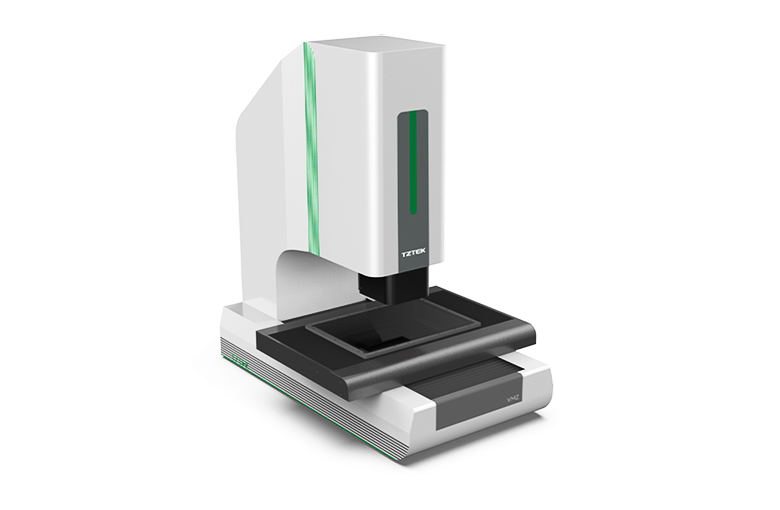
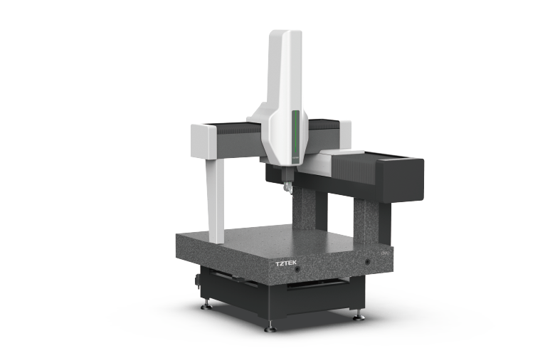
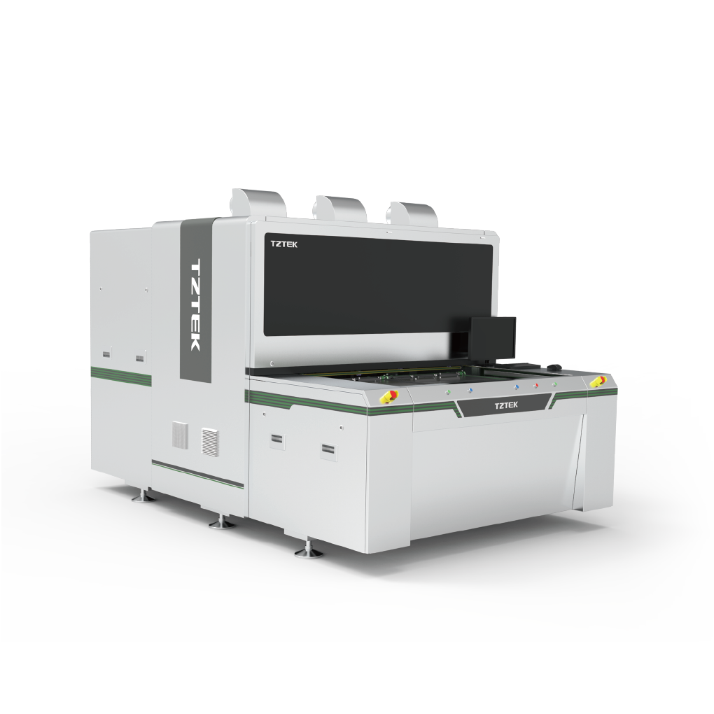
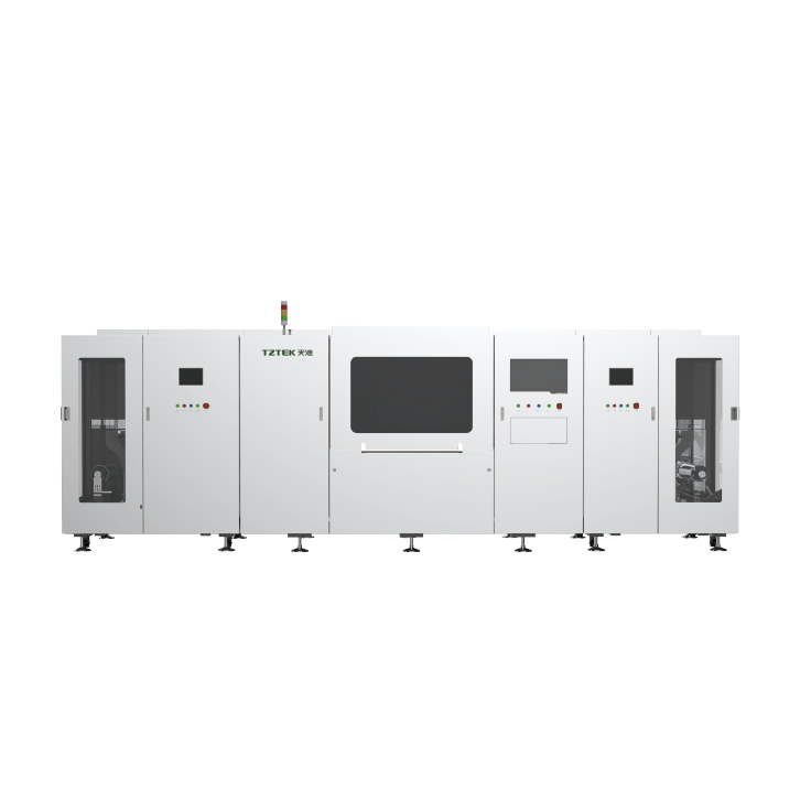
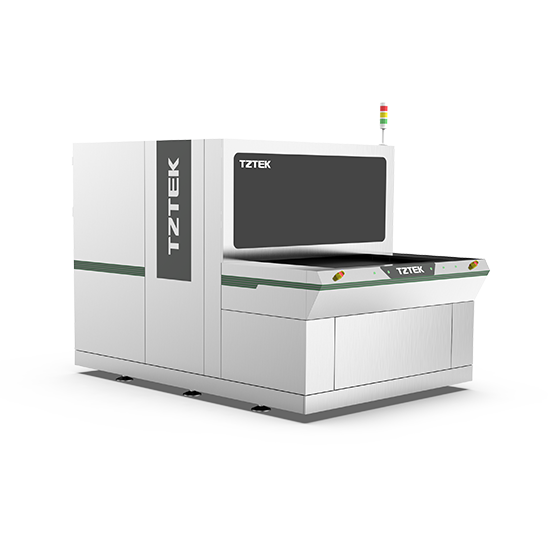
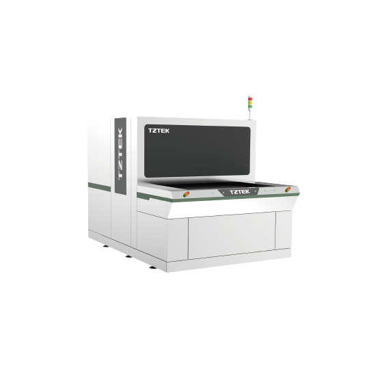
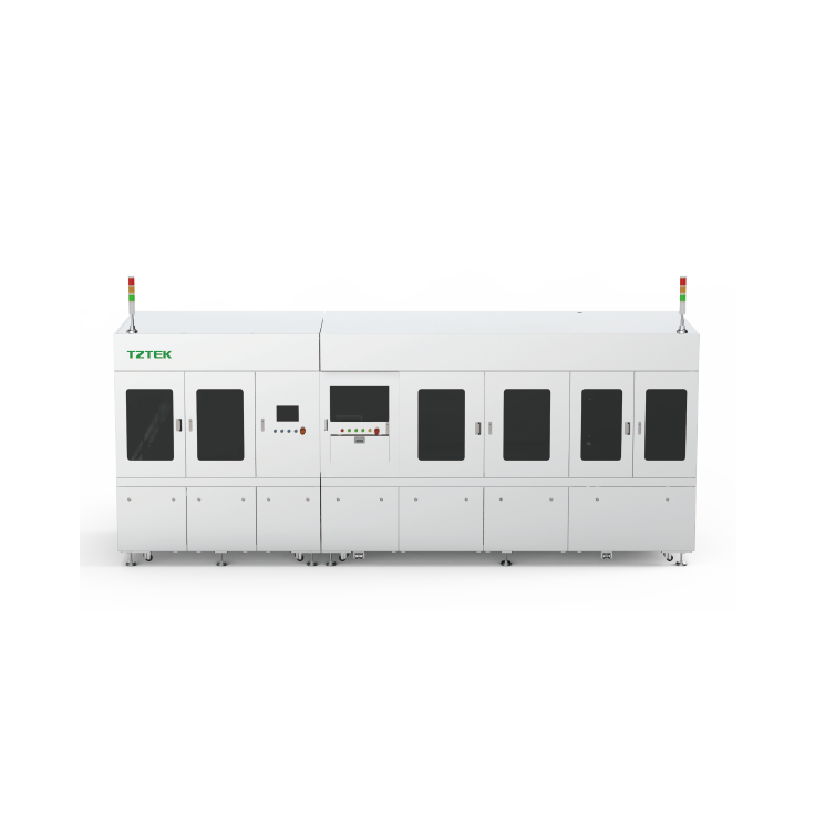
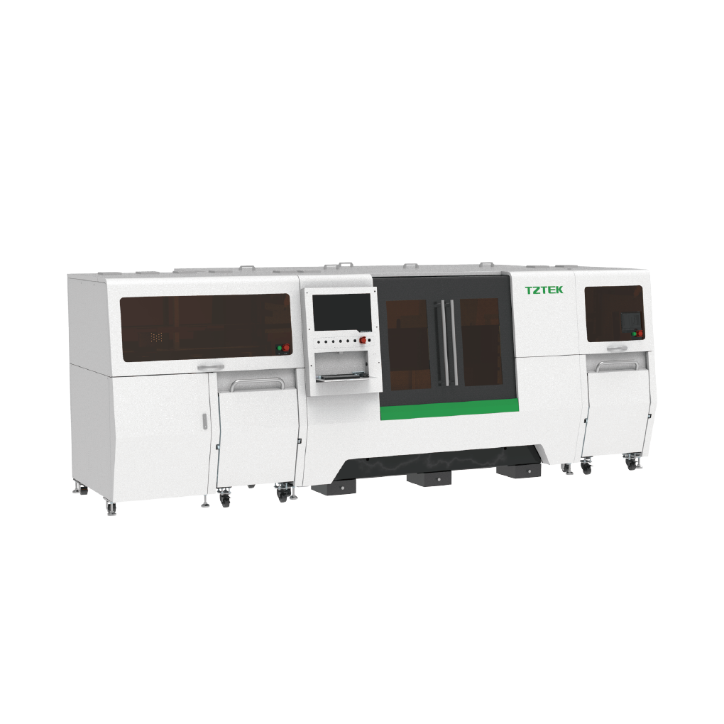
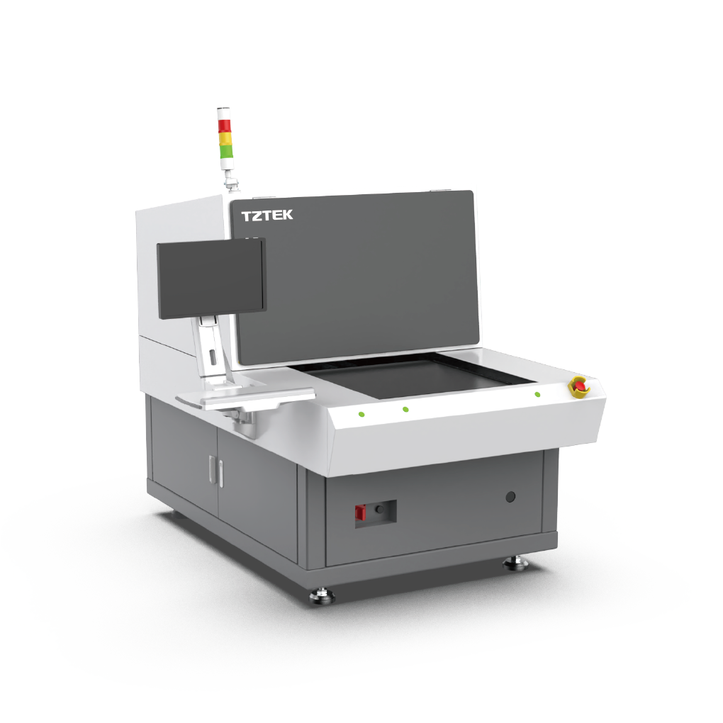
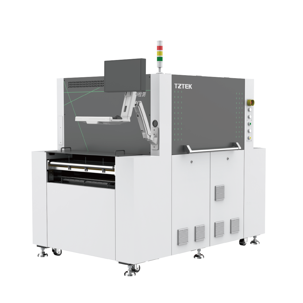
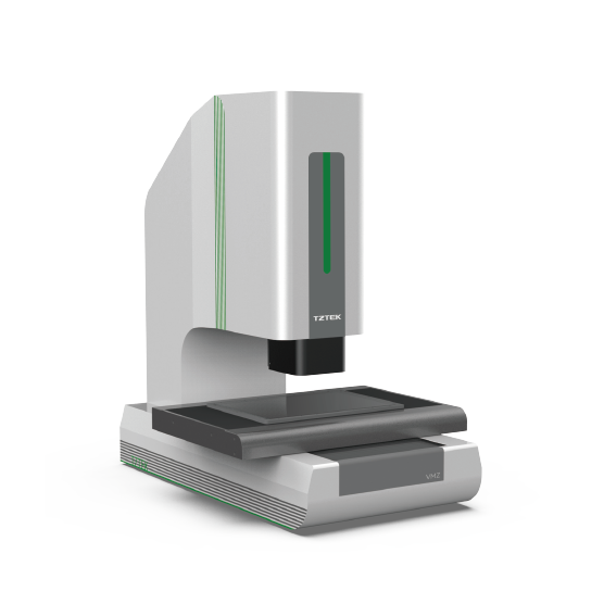
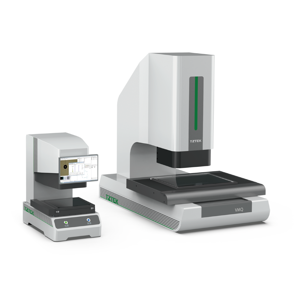
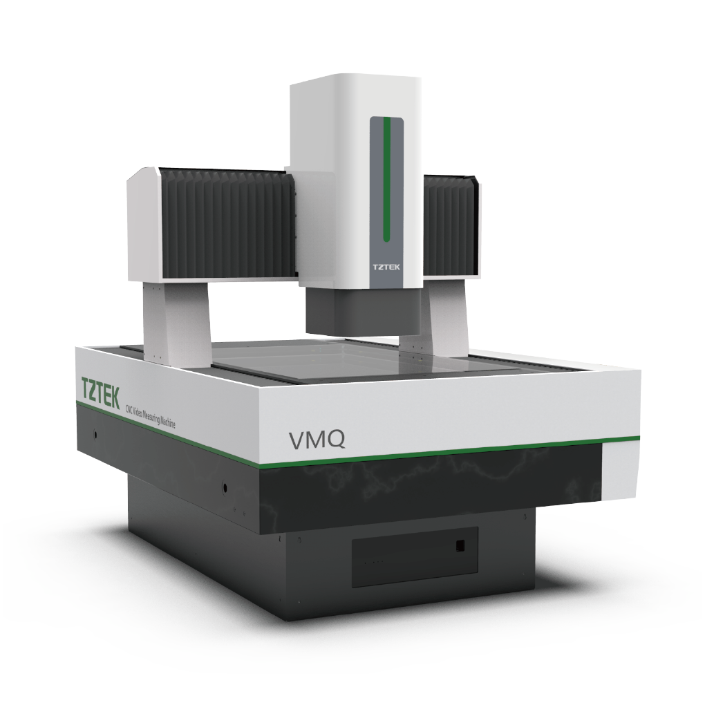
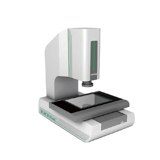
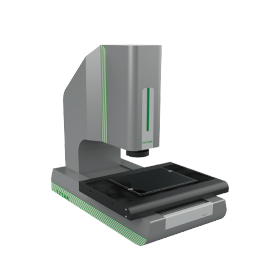
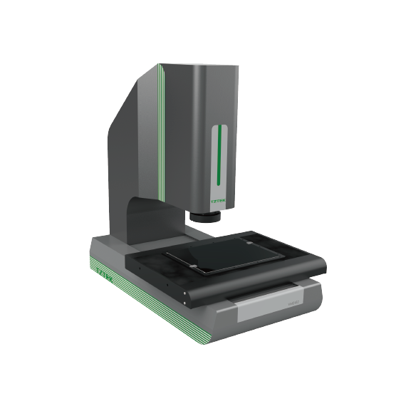
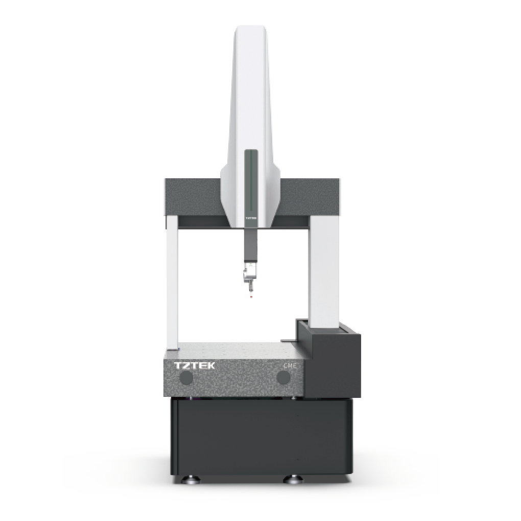
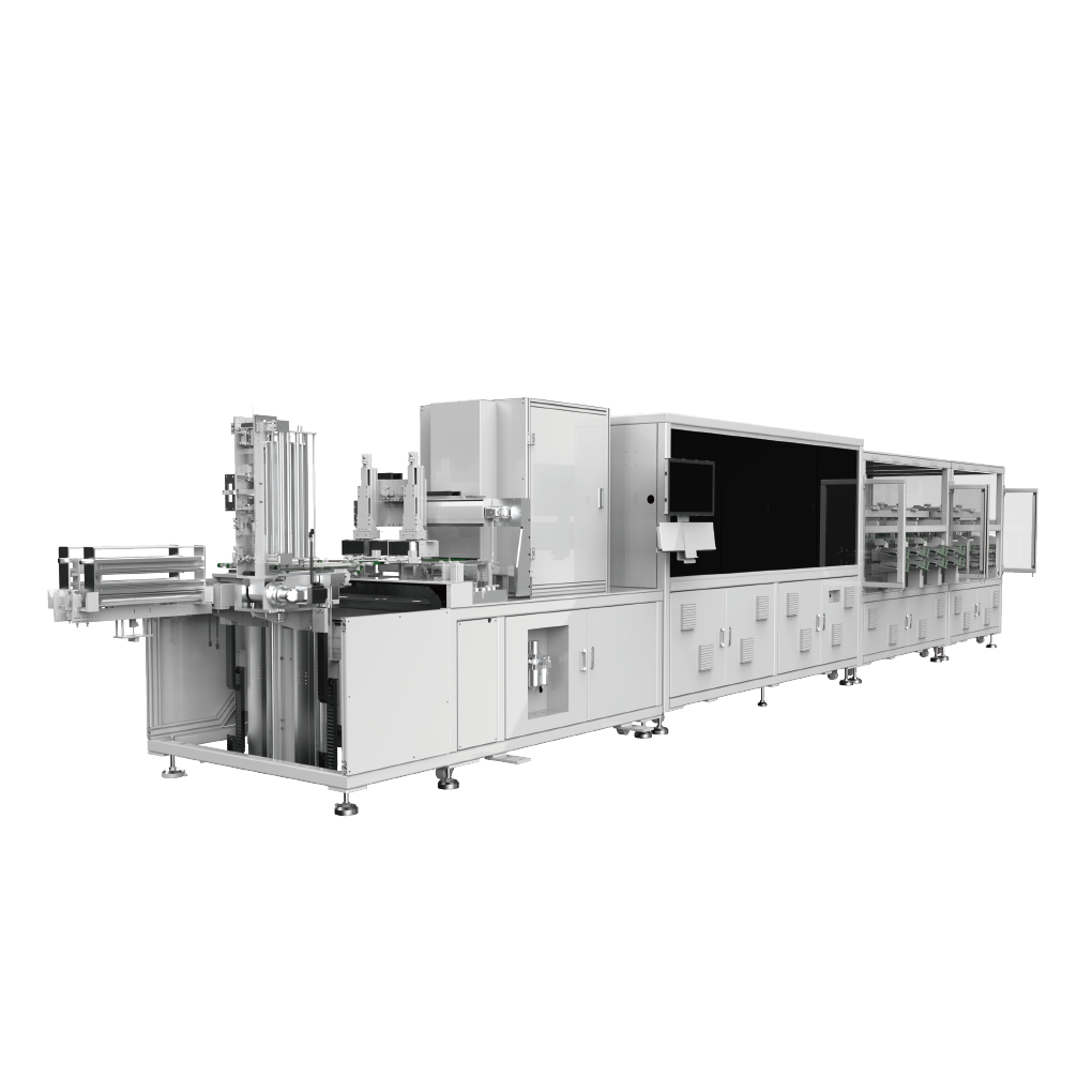
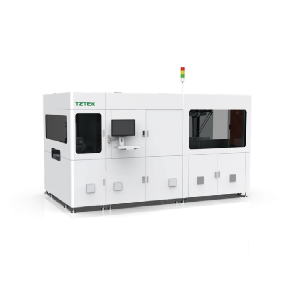
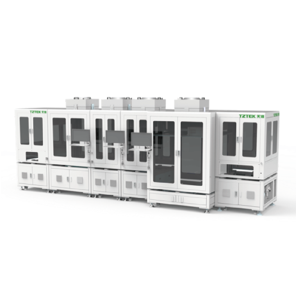
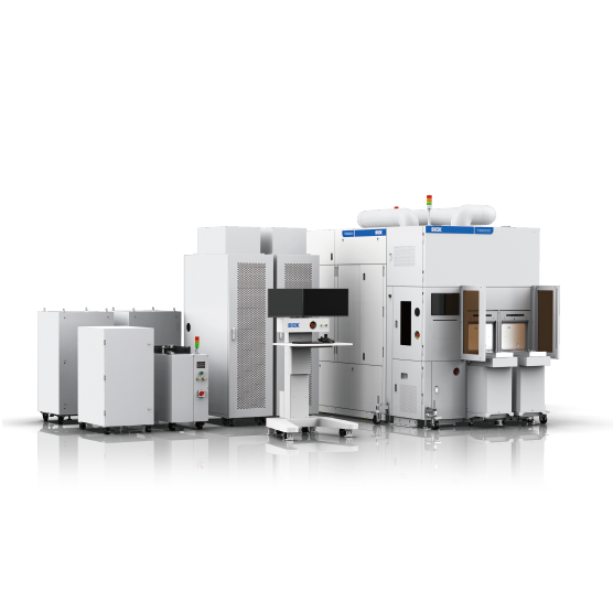
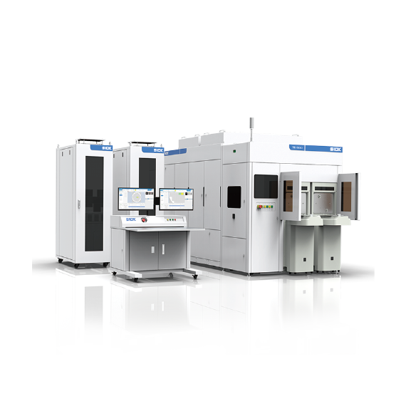
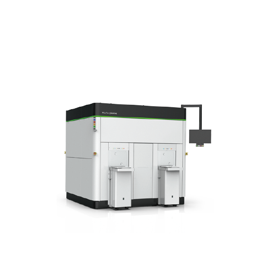
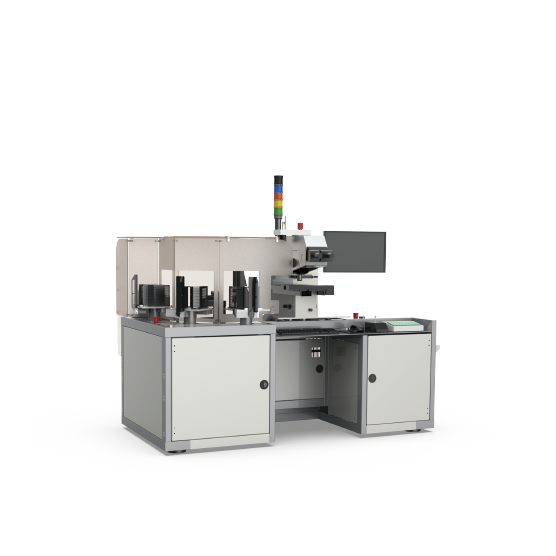
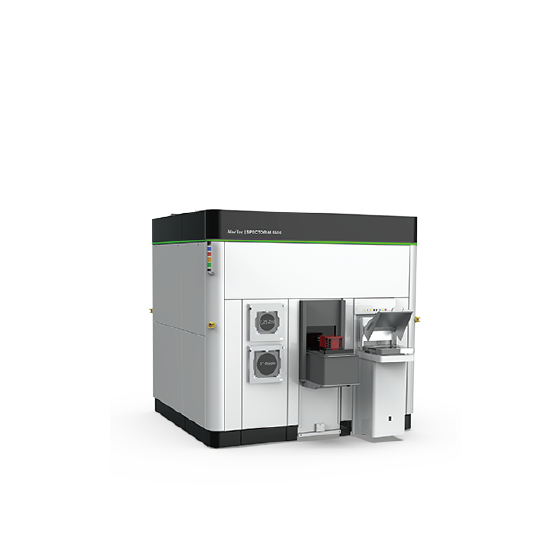
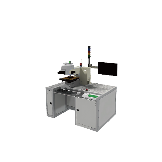
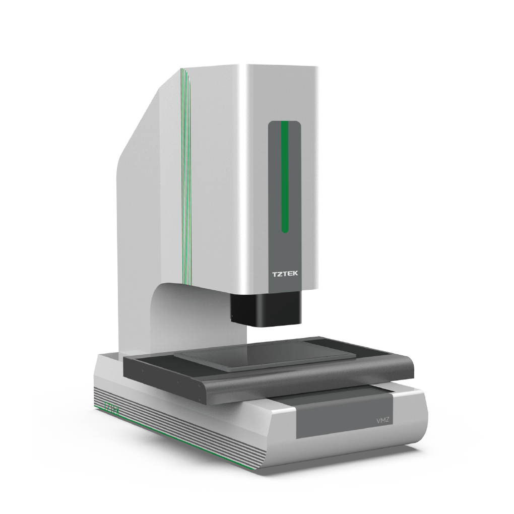
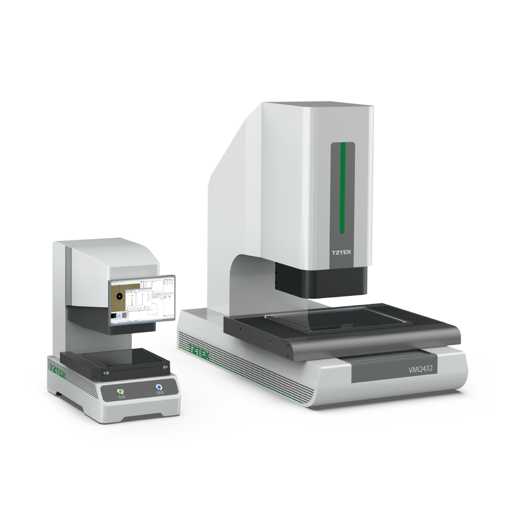
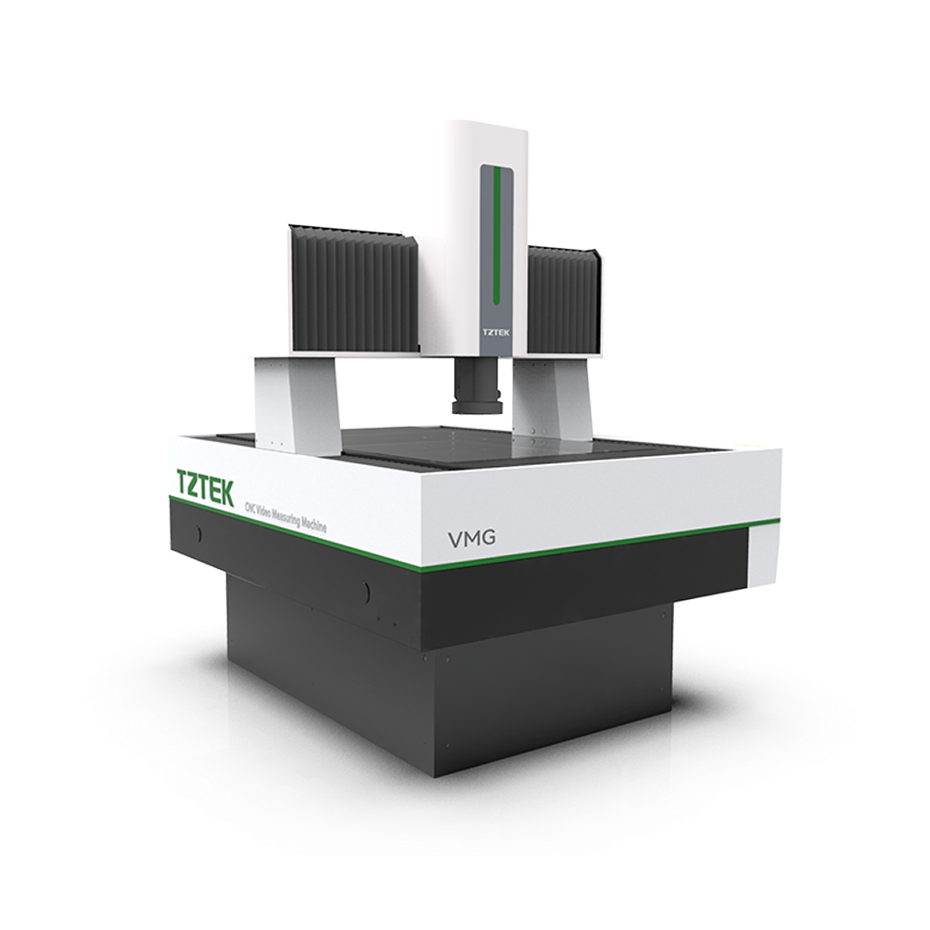
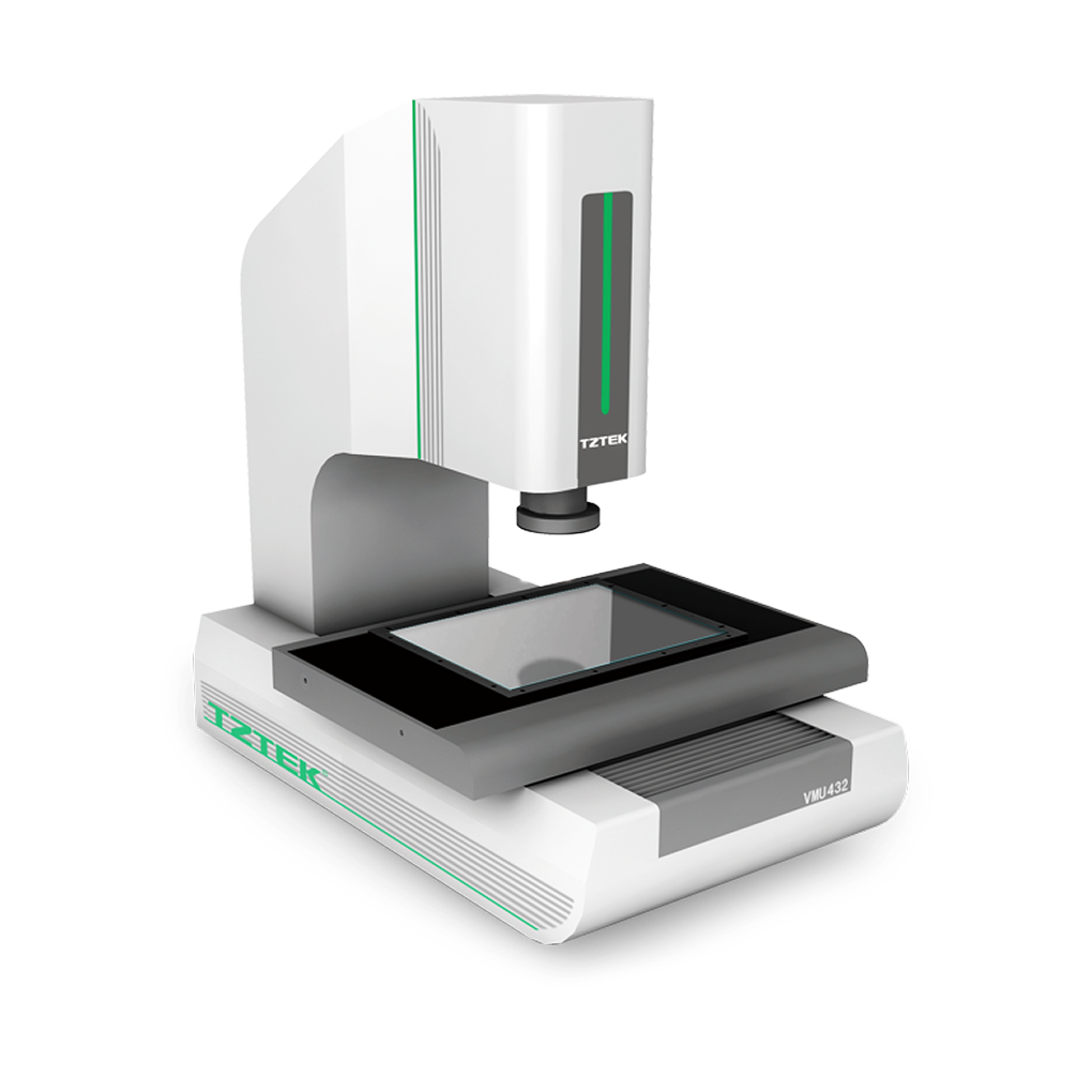
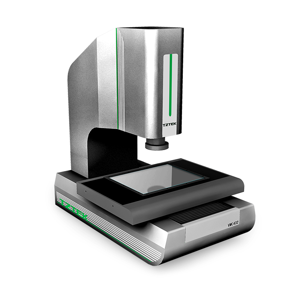
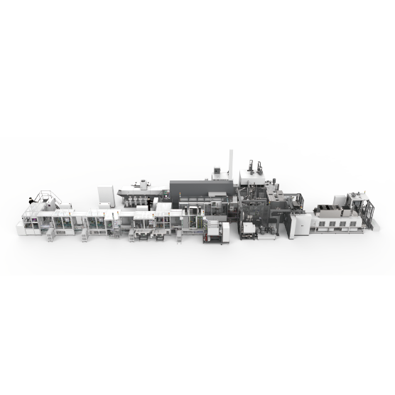
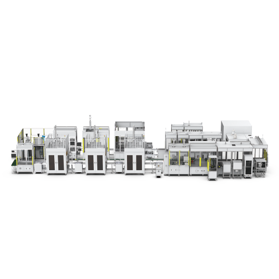
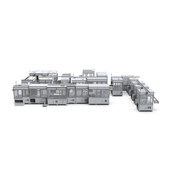
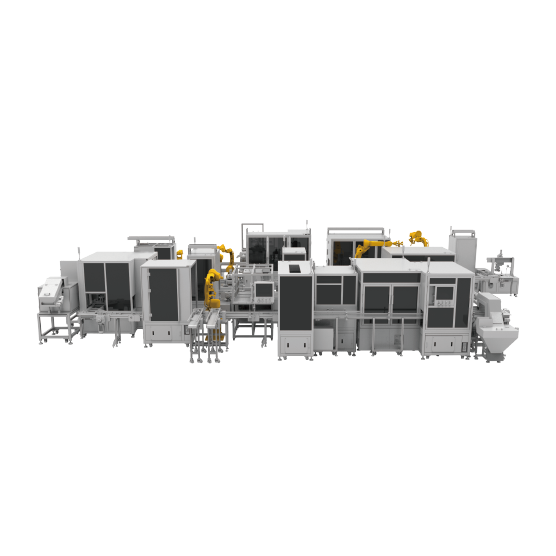
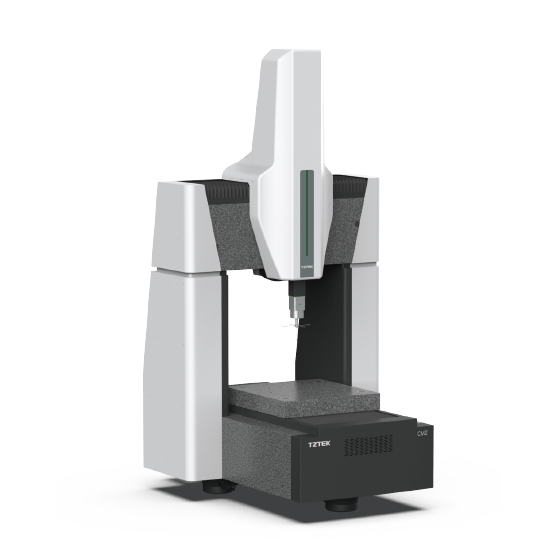
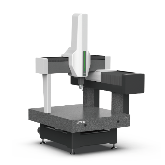
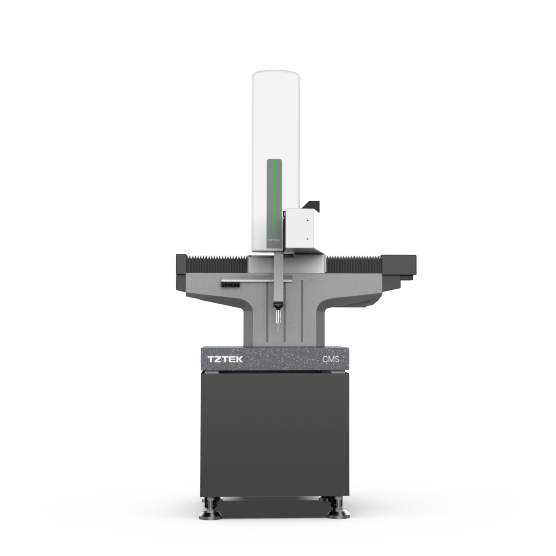
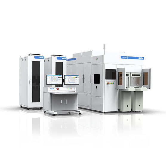
ADVANCED METROLOGY & INSPECTION SOLUTIONS
Pioneering Innovation, Relentless Progress
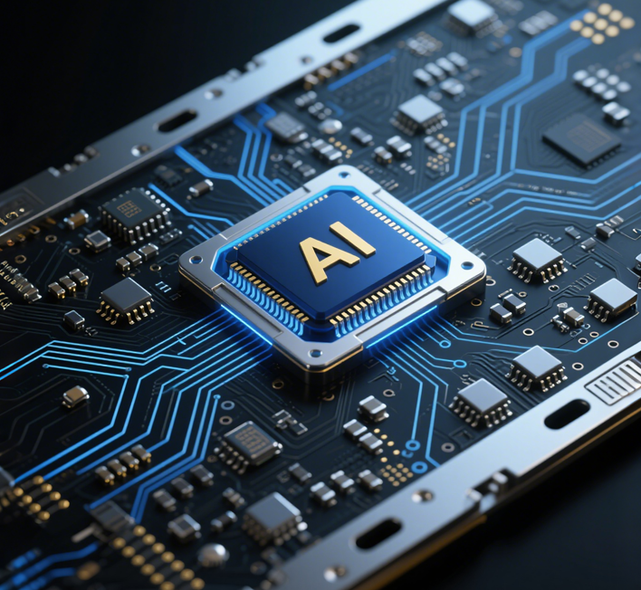
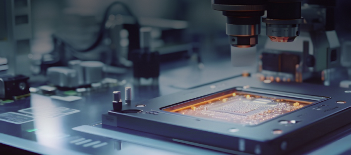
Ongoing high-investment in R&D, focusing on cutting-edge AI and optical metrology technologies, while continually pushing the limits of equipment precision and efficiency.
-

Precision Engineering, Empowering Our Clients
A team of senior process experts harnesses state-of-the-art equipment to provide comprehensive yield improvement solutions, delivering exceptional value to our customers.
-
Autonomous and Self-Sufficient, Serving a Global Market
Blending Chinese and German manufacturing expertise, mastering end-to-end autonomous technologies, driving China's industrial advancement, and supporting the global semiconductor industry.