


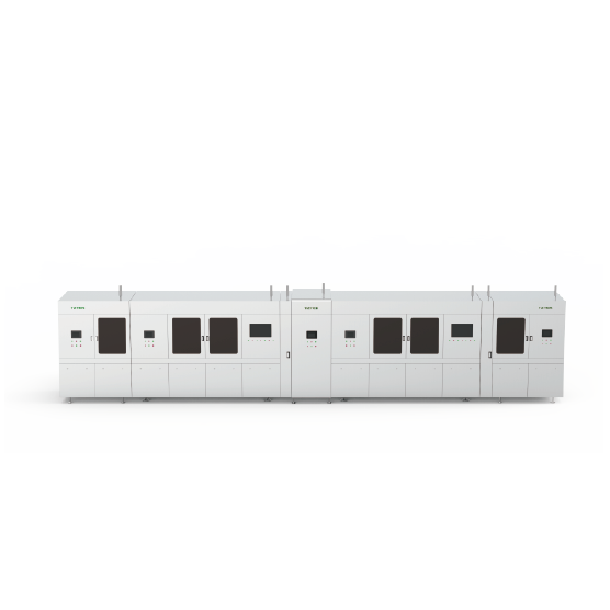
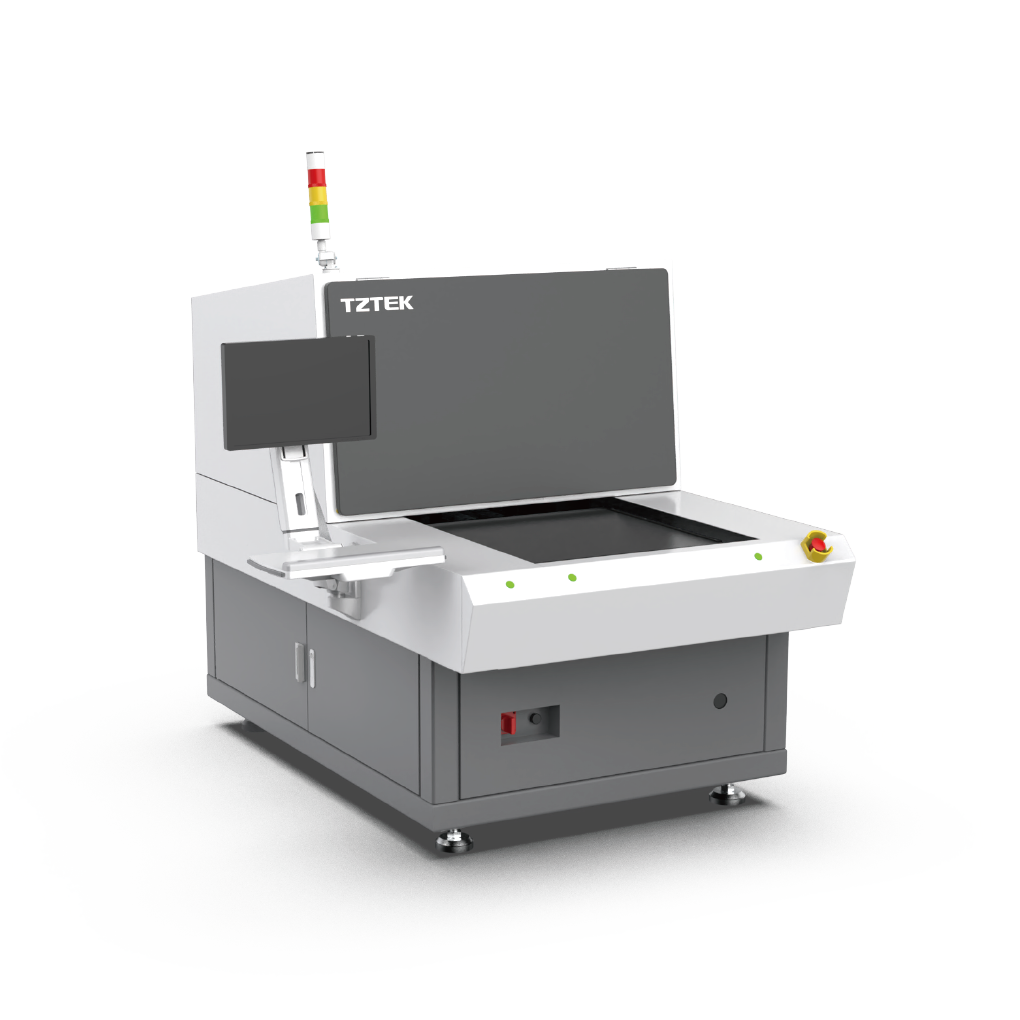
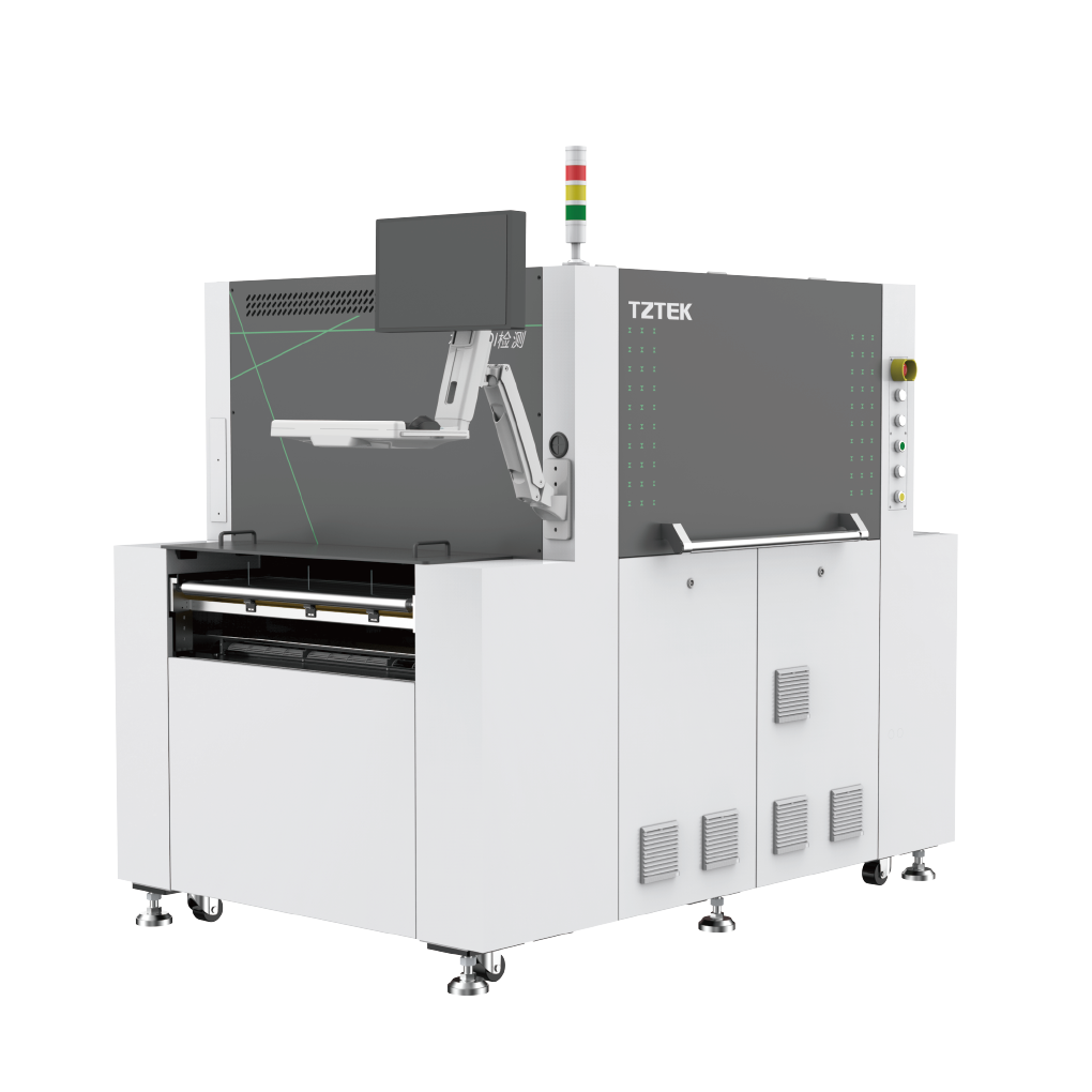
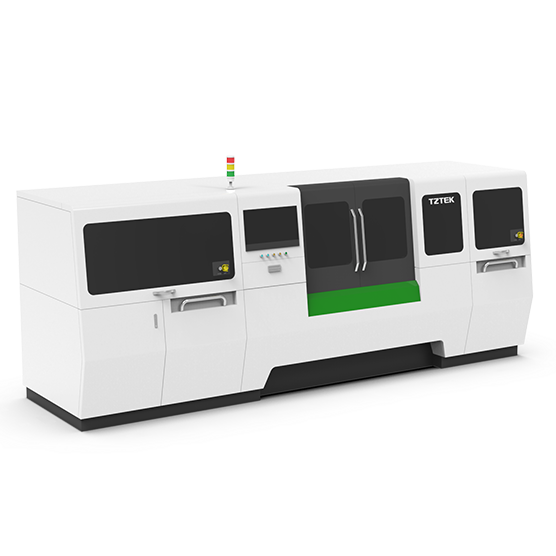
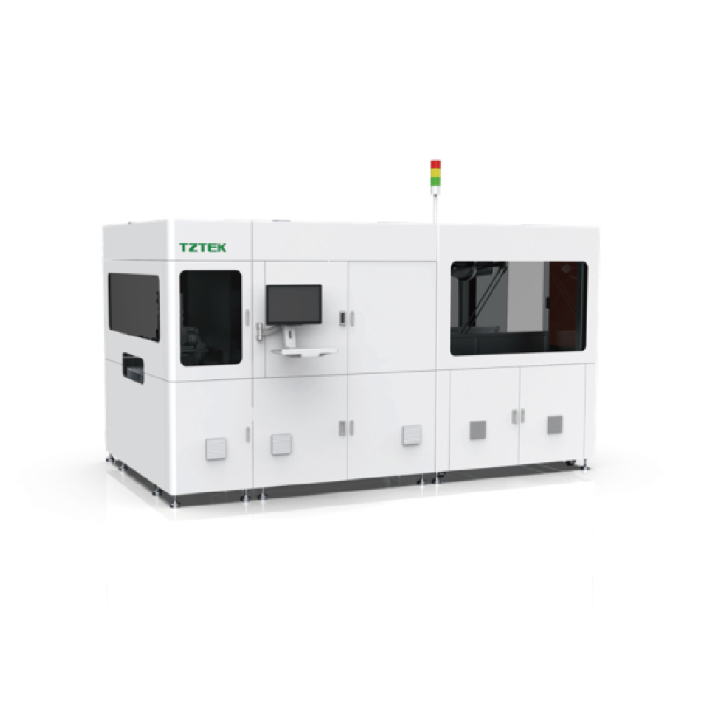
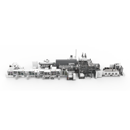
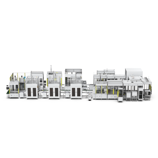
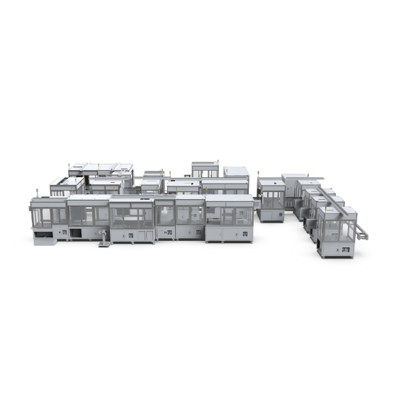
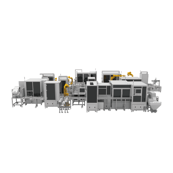
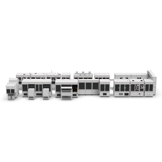
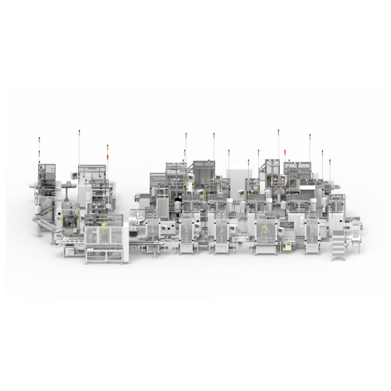
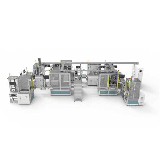
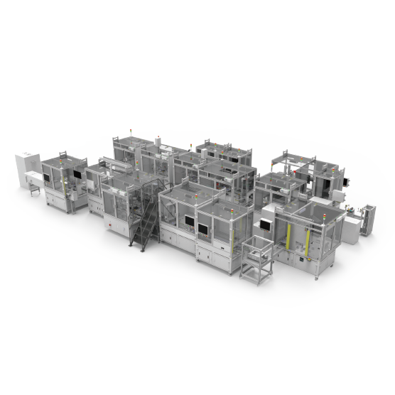
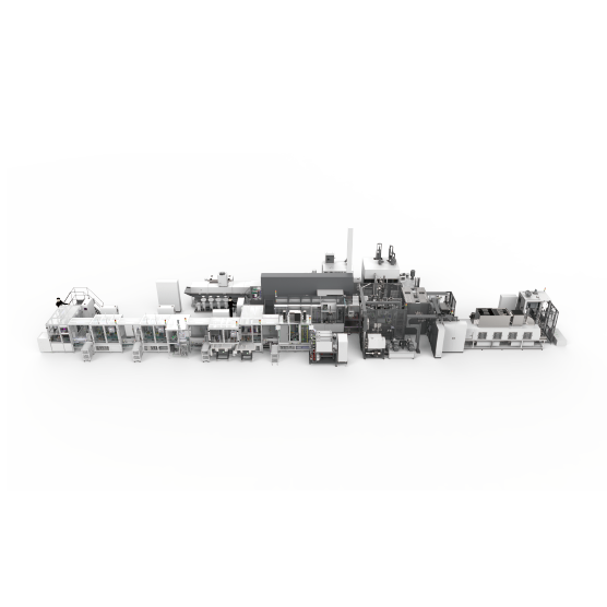
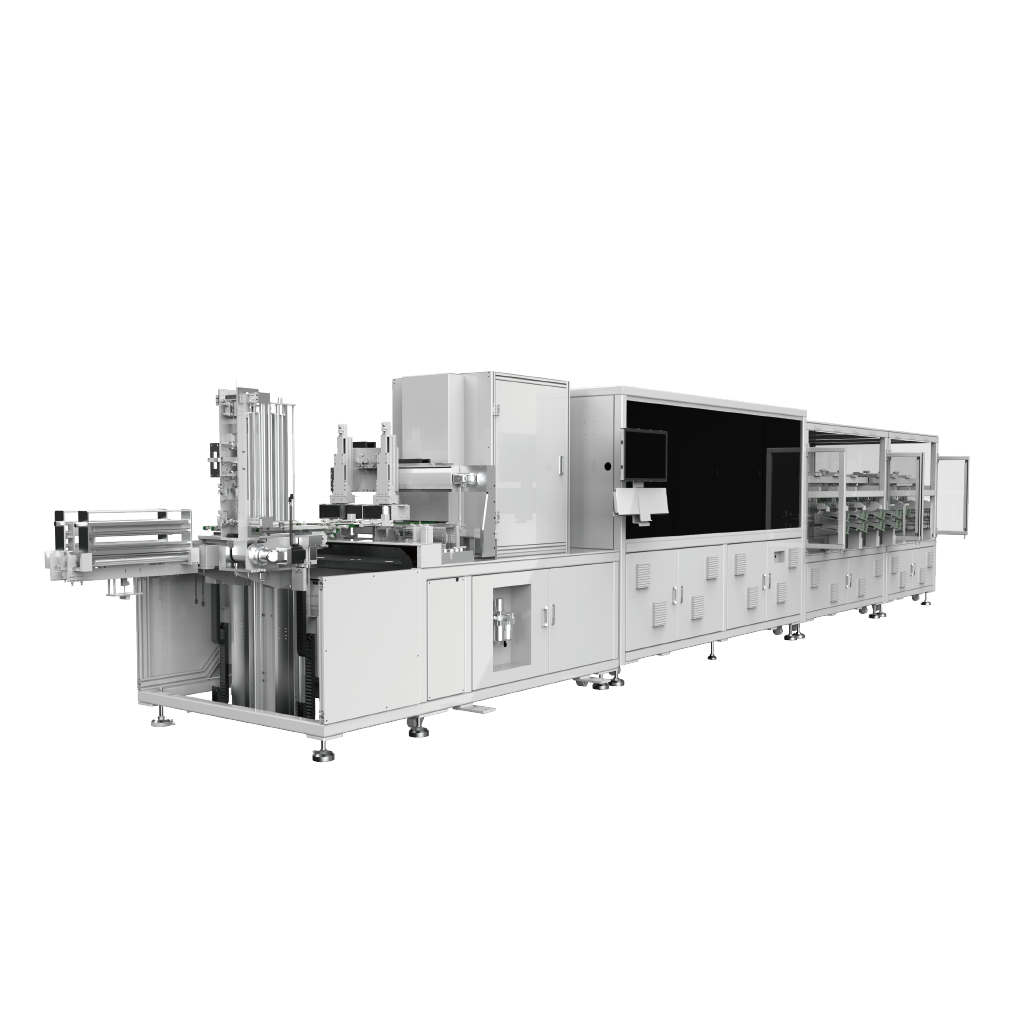




Inline Optical Inspection for PCB Manufacturing
INDUSTRY CHALLENGES
-
 01
01Full PCB inspection is becoming the industry standard, making manual inspection increasingly costly and difficult to scale.
-
02
Conventional AOI systems often generate high false-call rates, increasing review workload and risking missed defects.
-
03
Frequent product mix and part-number changes require manual program creation and adjustment, reducing overall inspection efficiency.


INDUSTRY SOLUTION
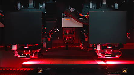
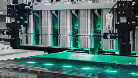
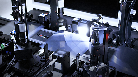
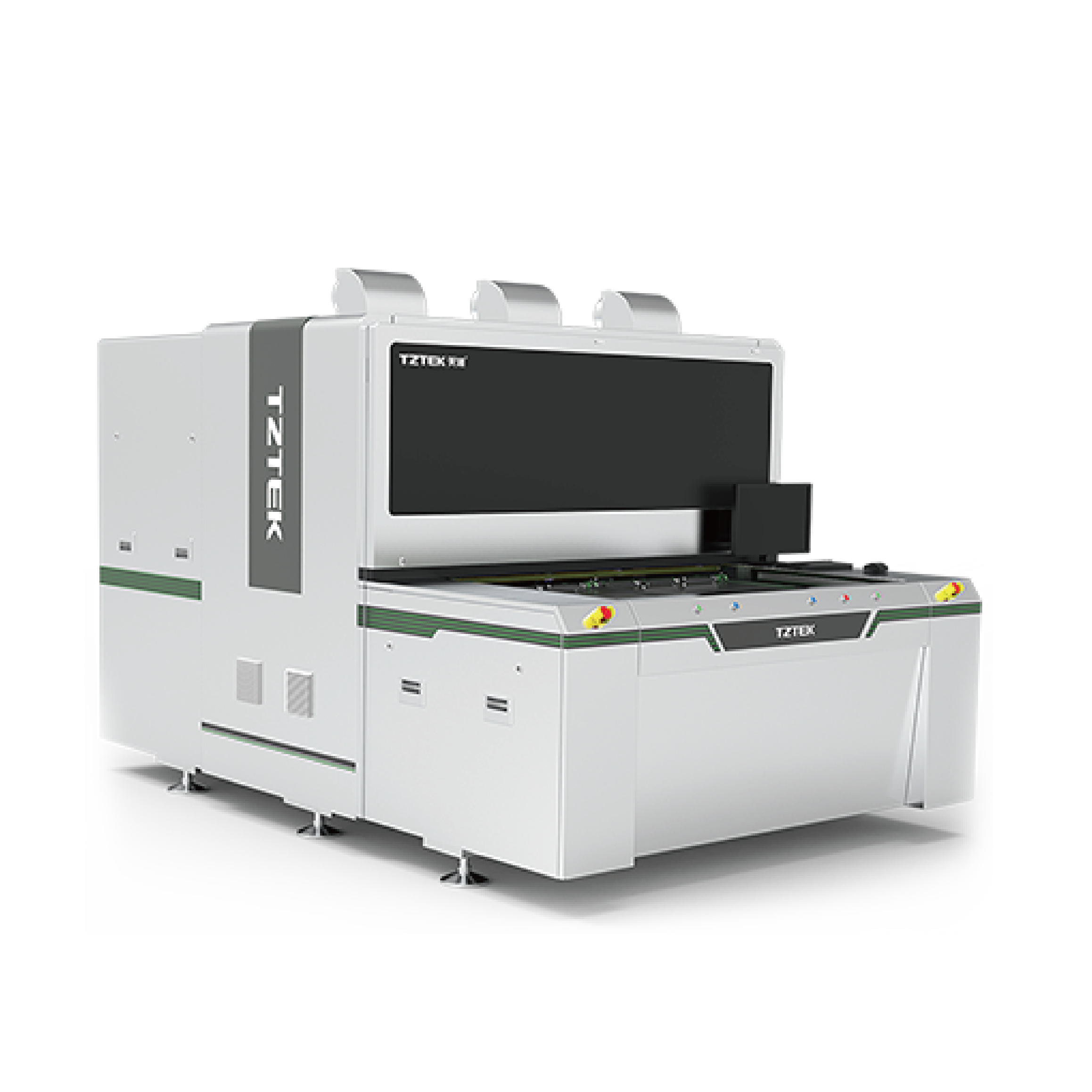
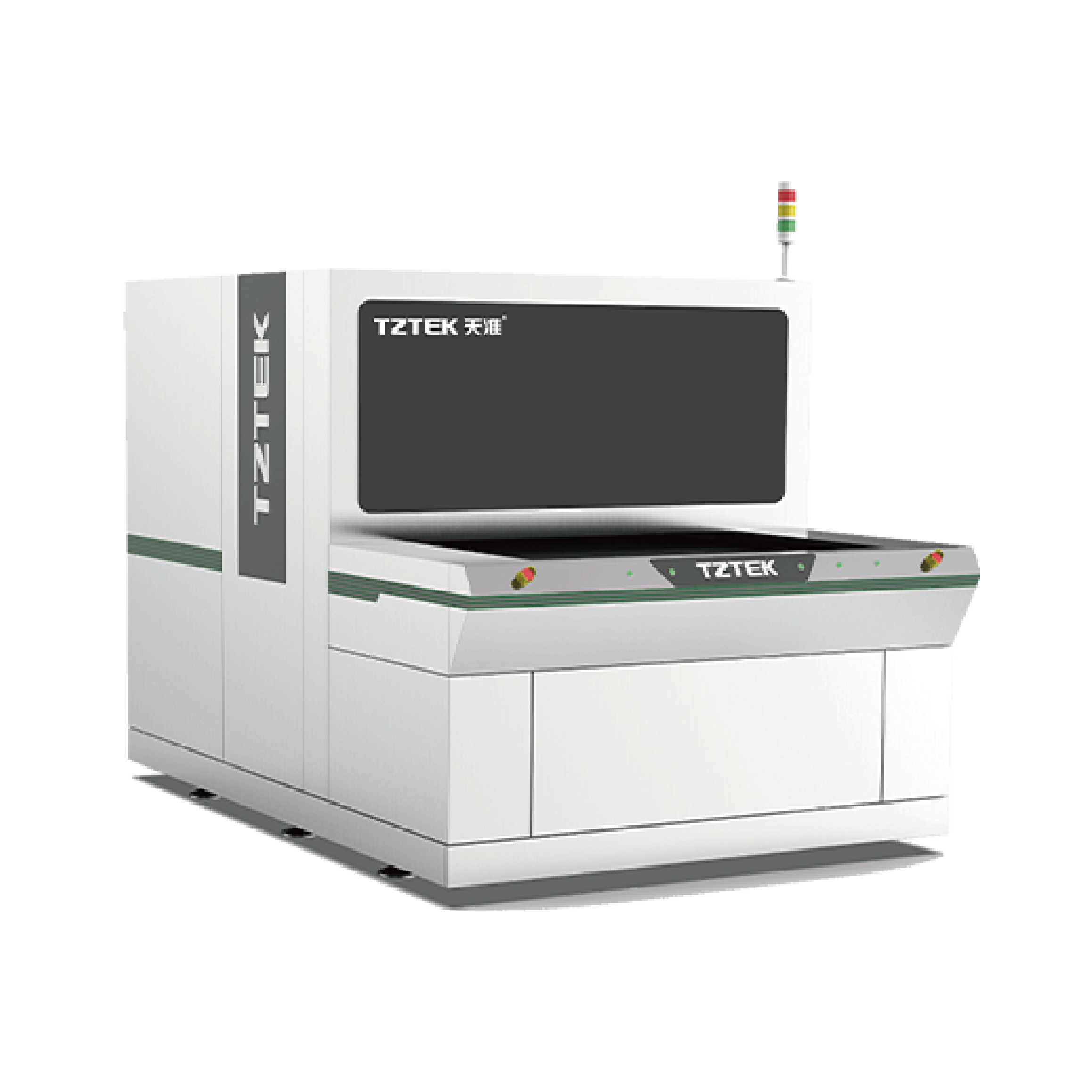
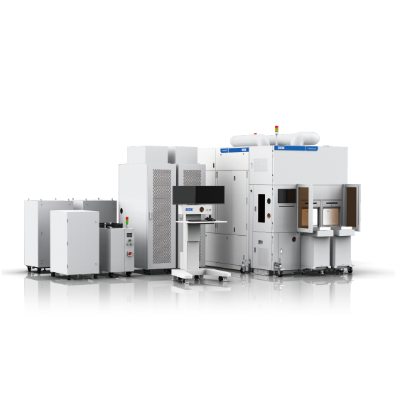
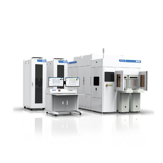
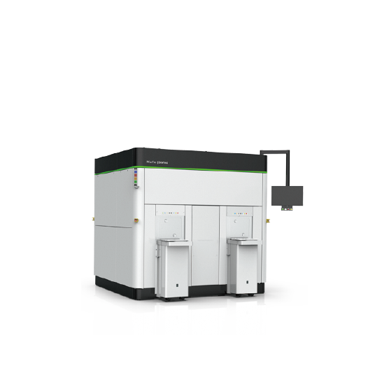
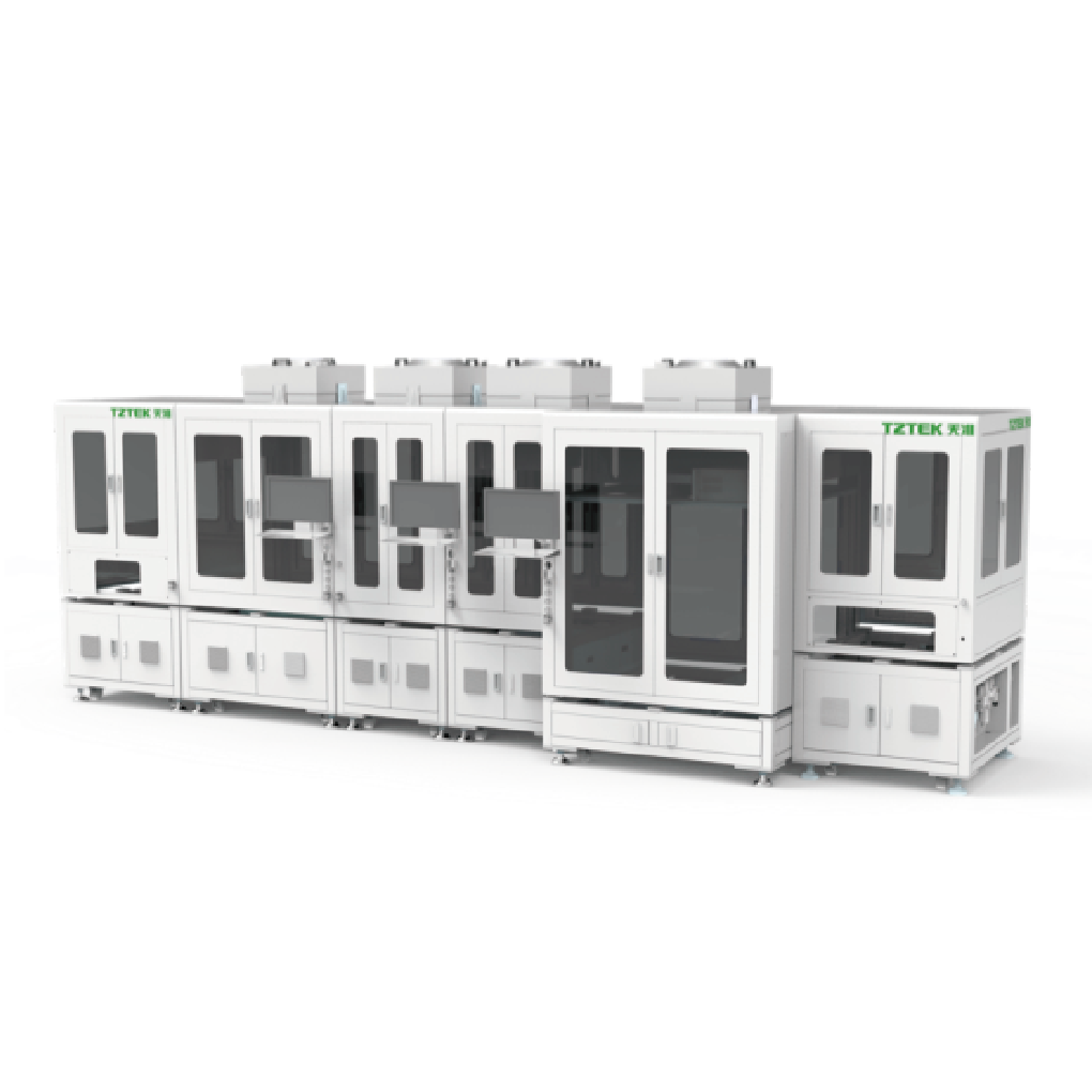
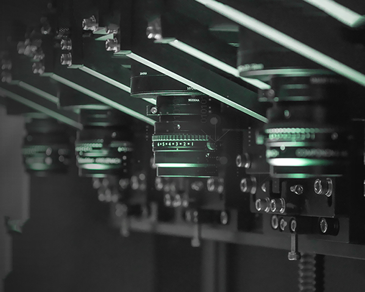
TZTEK's AOI combines a water-cooled, high-intensity multispectral optical system with a 16K color TDI line-scan camera to deliver high-resolution defect imaging.
Sub-pixel edge extraction delivers precise edge profiles for reliable geometric measurement and defect classification, minimizing stair-step artifacts.
CAM-based pattern-edge comparison and sub-pixel image analysis enhance sensitivity to subtle defects, enabling detection of fine edge deviations below the physical pixel resolution.
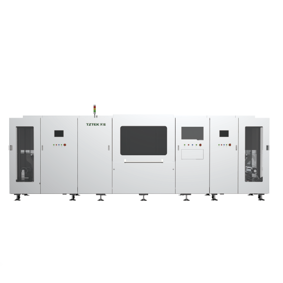
A modular architecture separates motion control, image acquisition, and inspection processing, ensuring stable 24/7 operation on etching lines.
High-performance computing provides reliable local image storage and scalable inspection capacity through additional inspection stations.
KEY ADVANTAGES
-


Independent motion control keeps the line running during software faults.
-

Image-based autofocus system ensures stable and sharp image capture.
-

AI-based false-call filtering reduces operator intervention by ≥90%.