


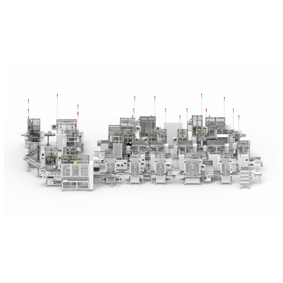
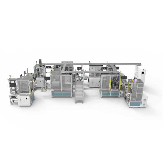
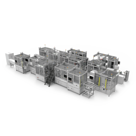
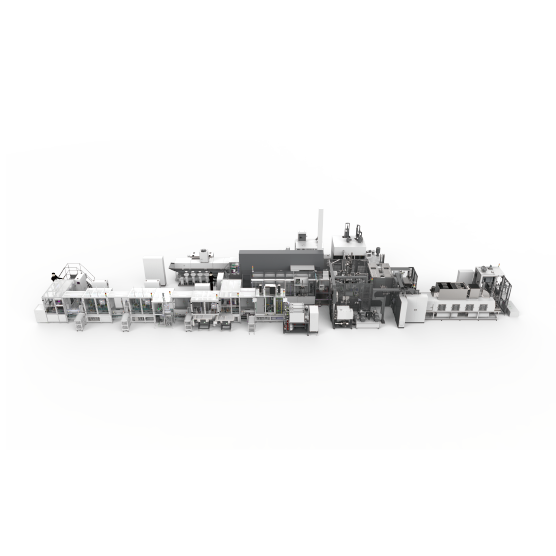




Brightfield Inspection
INDUSTRY SOLUTION
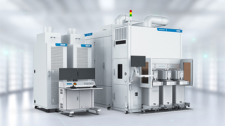
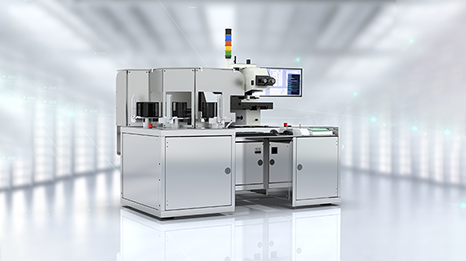
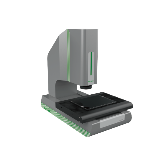
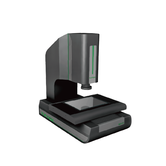
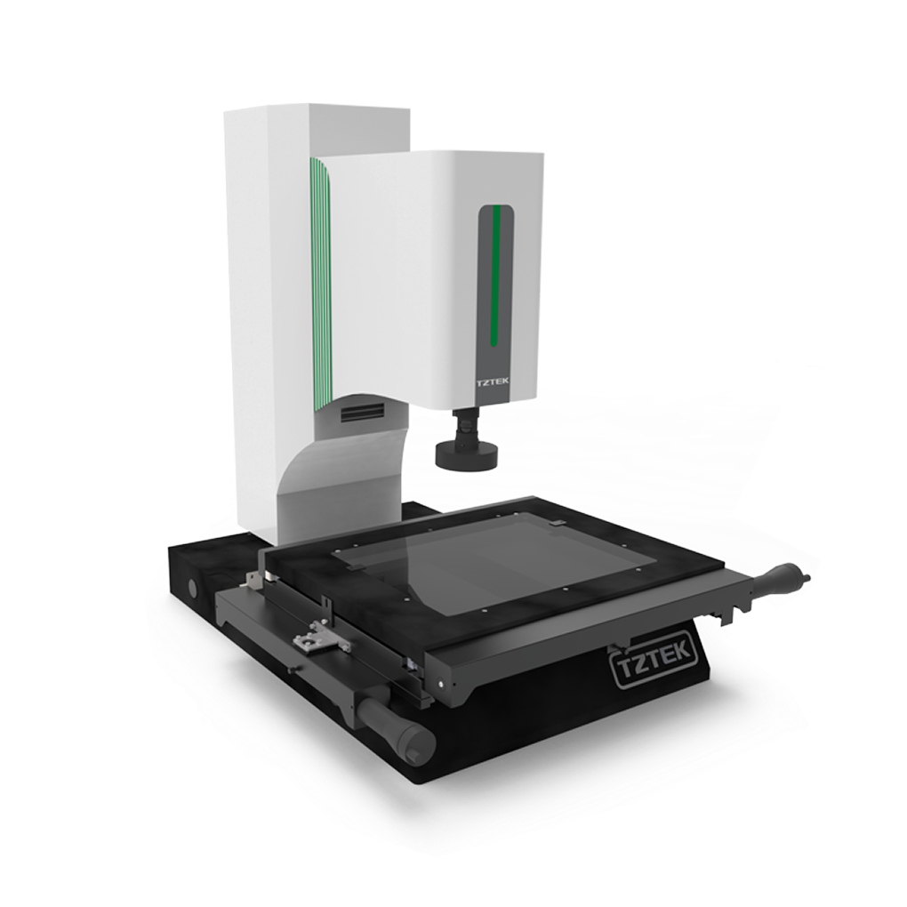
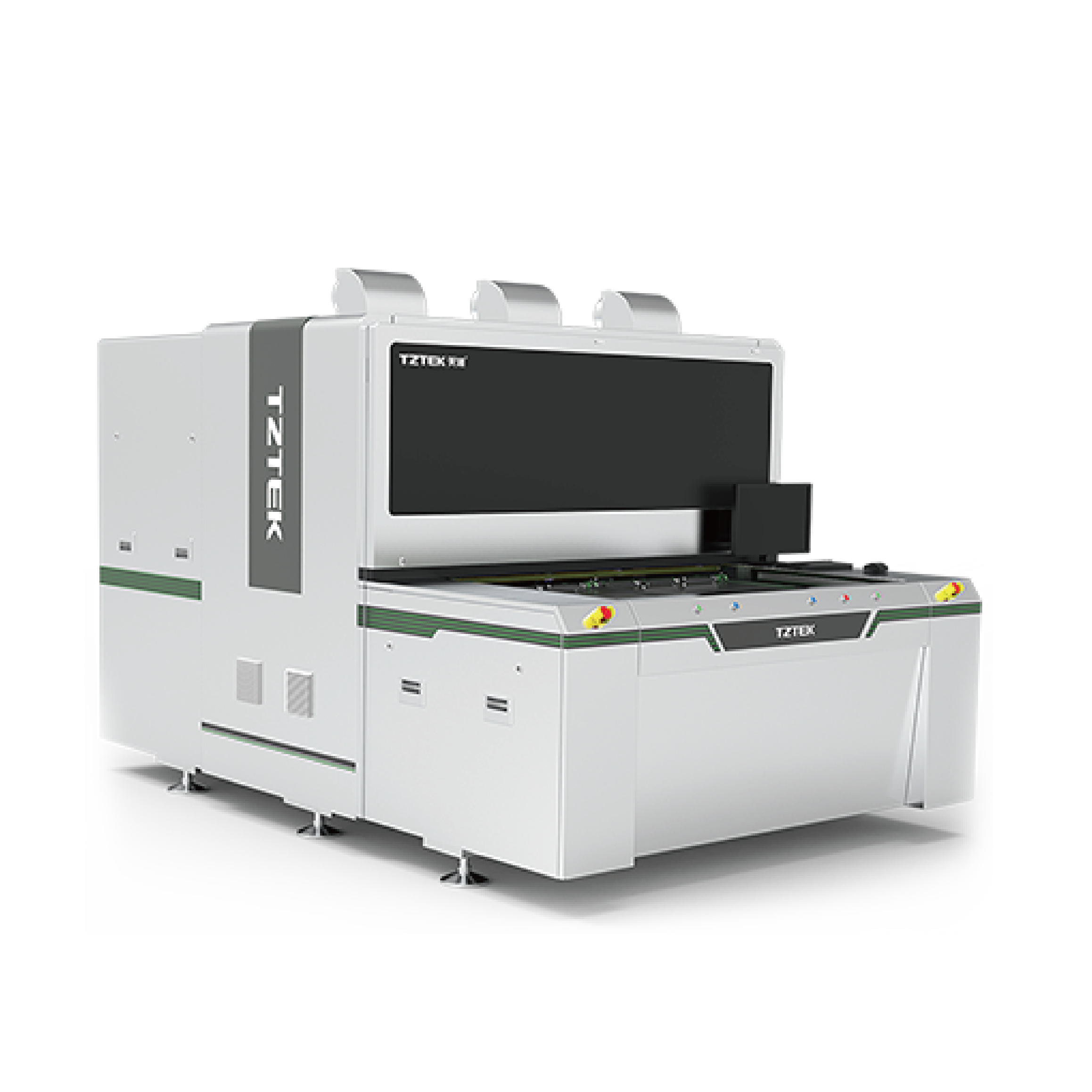
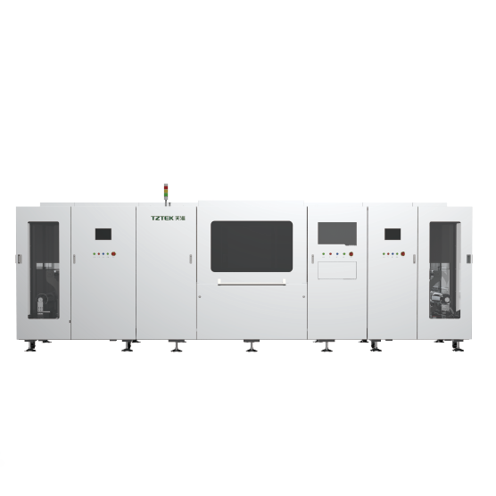
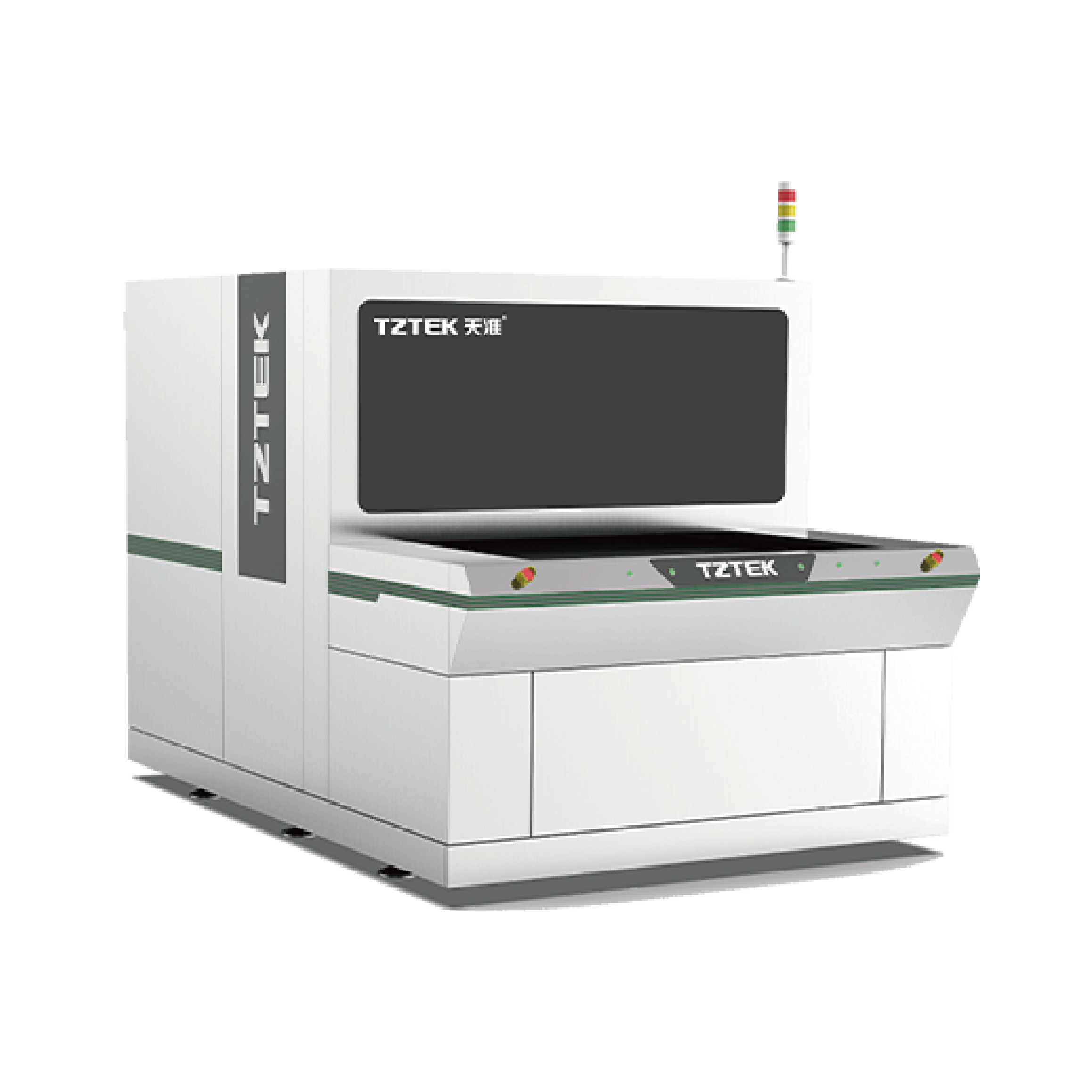
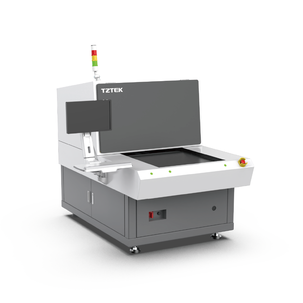
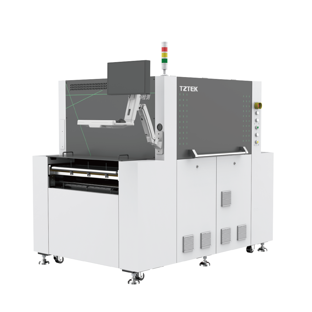
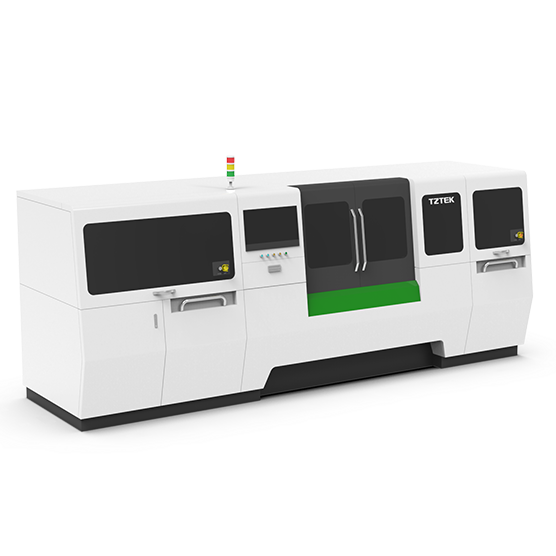
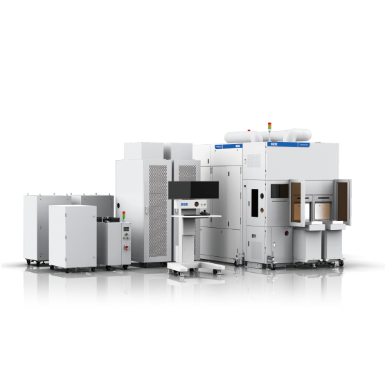
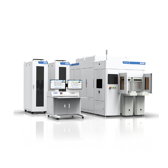
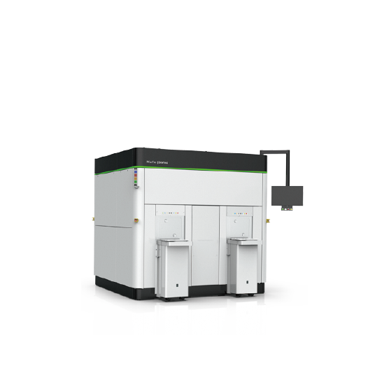
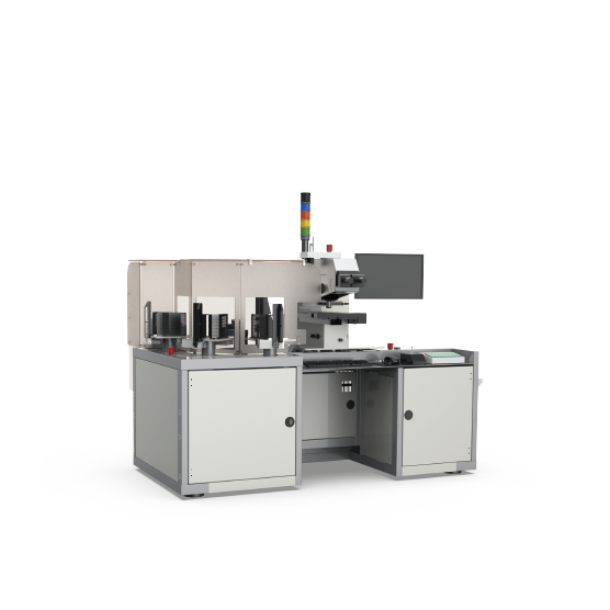
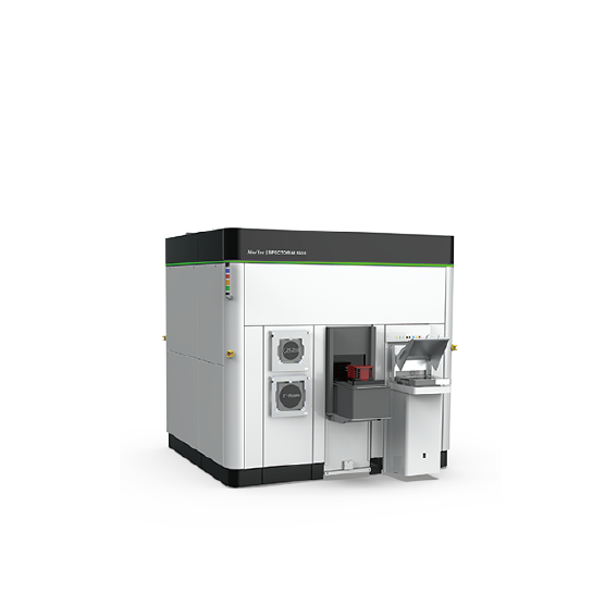
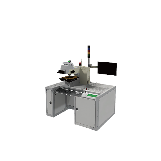
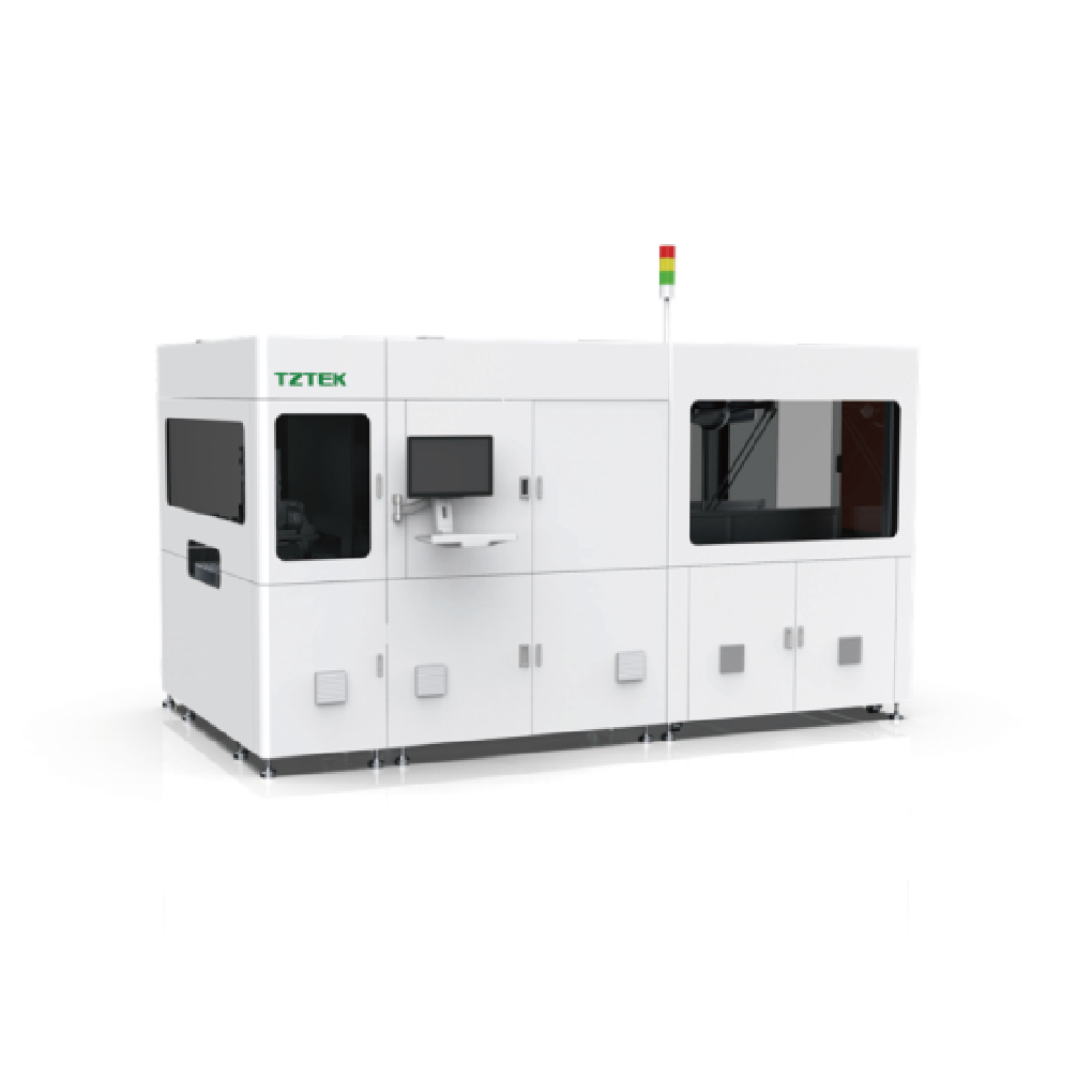
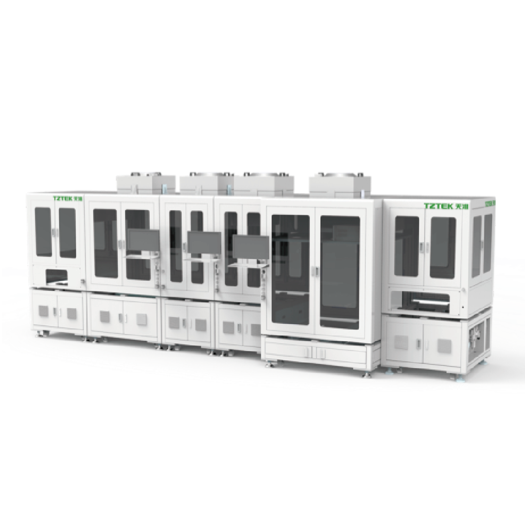
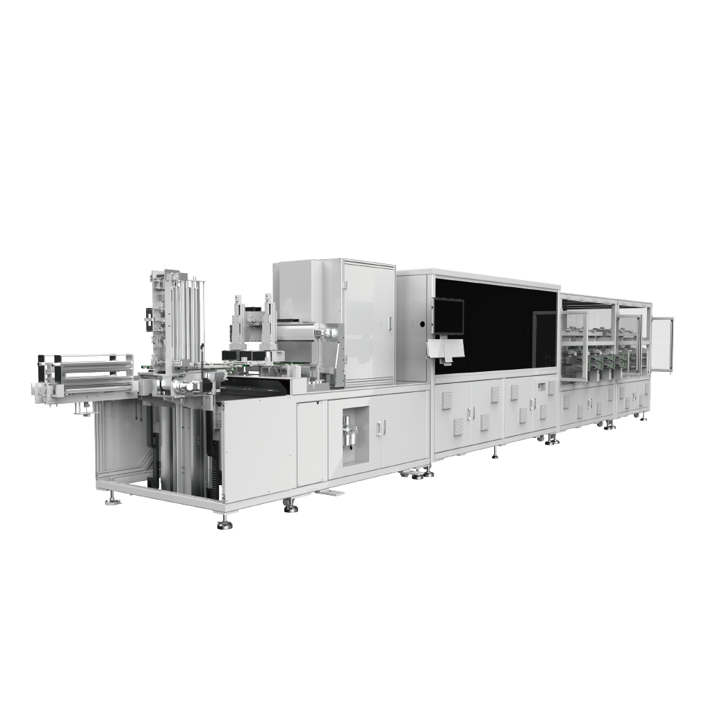
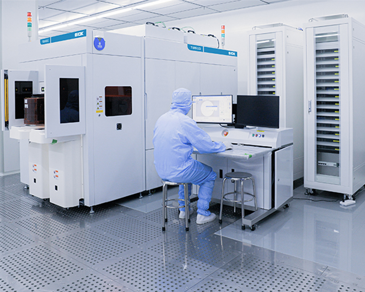
To address the inspection challenges of advanced packaging, TZTEK's brightfield inspection solution is optimized across hardware and software to support inspection of high-thickness, highly warped wafers with robust wafer handling and chucking.
The system features a long-travel Z-axis stage and an extended focus range, improving defect detection within thick film layers.
The system supports multi-material optical simulation and full-wave time-domain simulation based on actual process structures, covering wavelengths from 260–600 nm to optimize inline inspection.
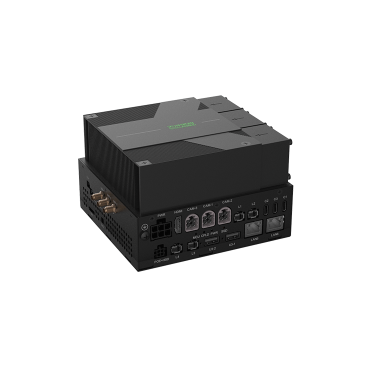
A high-speed motion stage synchronizes continuous motion with TDI to reduce step-and-settle time. Combined with HPC, it accelerates data processing and improves overall inspection efficiency.
KEY ADVANTAGES
-


AI Algorithms & Data Analytics: Intelligent inspection, noise suppression, and support for diverse applications.
-

High-Speed Motion stage: Faster motion improves overall inspection throughput.
-

Extended Focus Range: Long-travel Z-axis supports a wide range of focus positions.
-

Long-Travel Stage: Long Z-axis travel with adaptive zoned wafer chucking, supporting high-thickness and highly warped wafers.