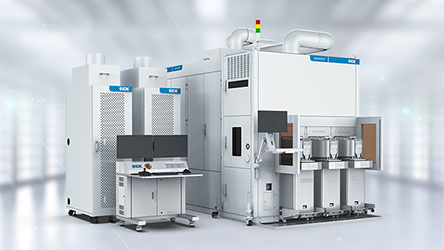



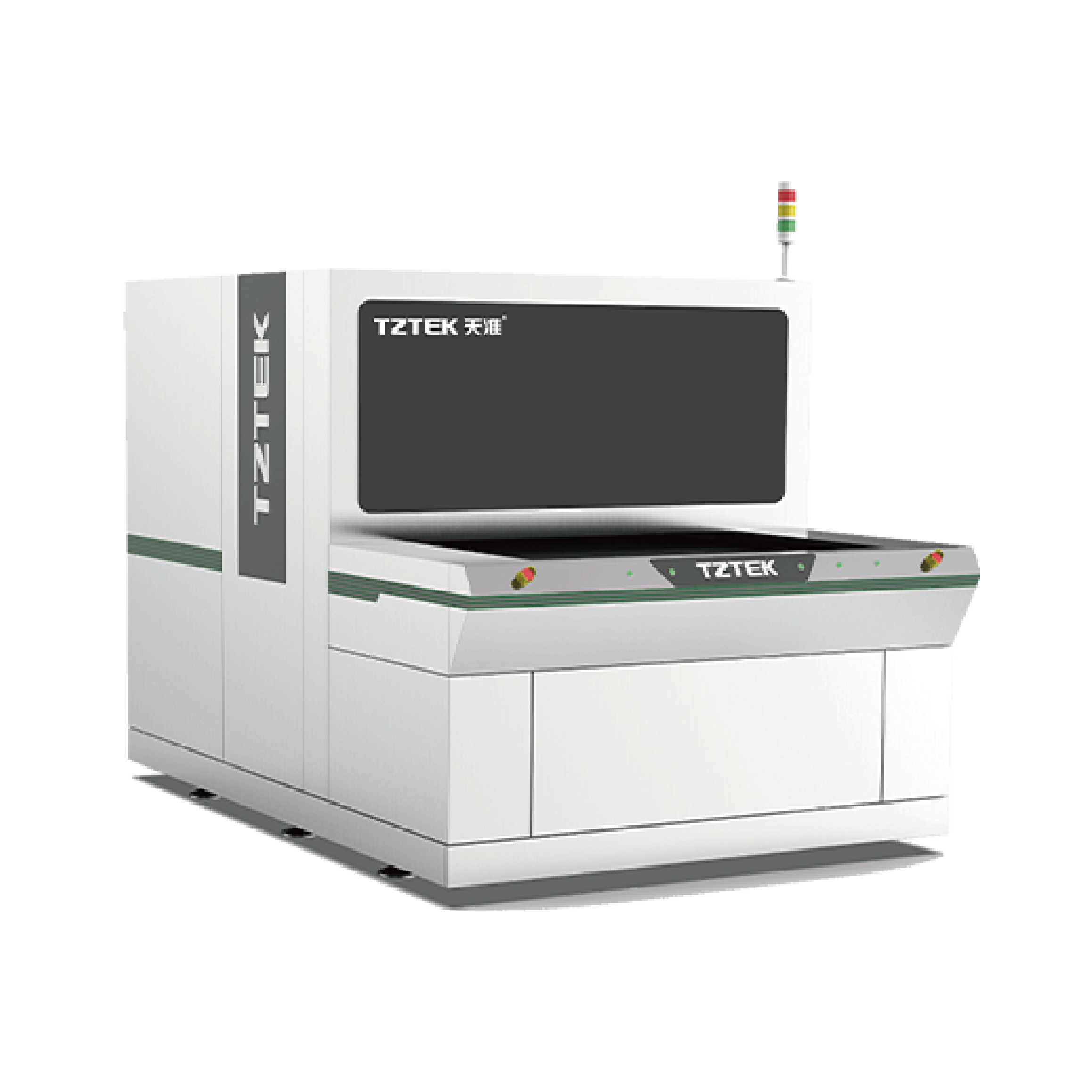
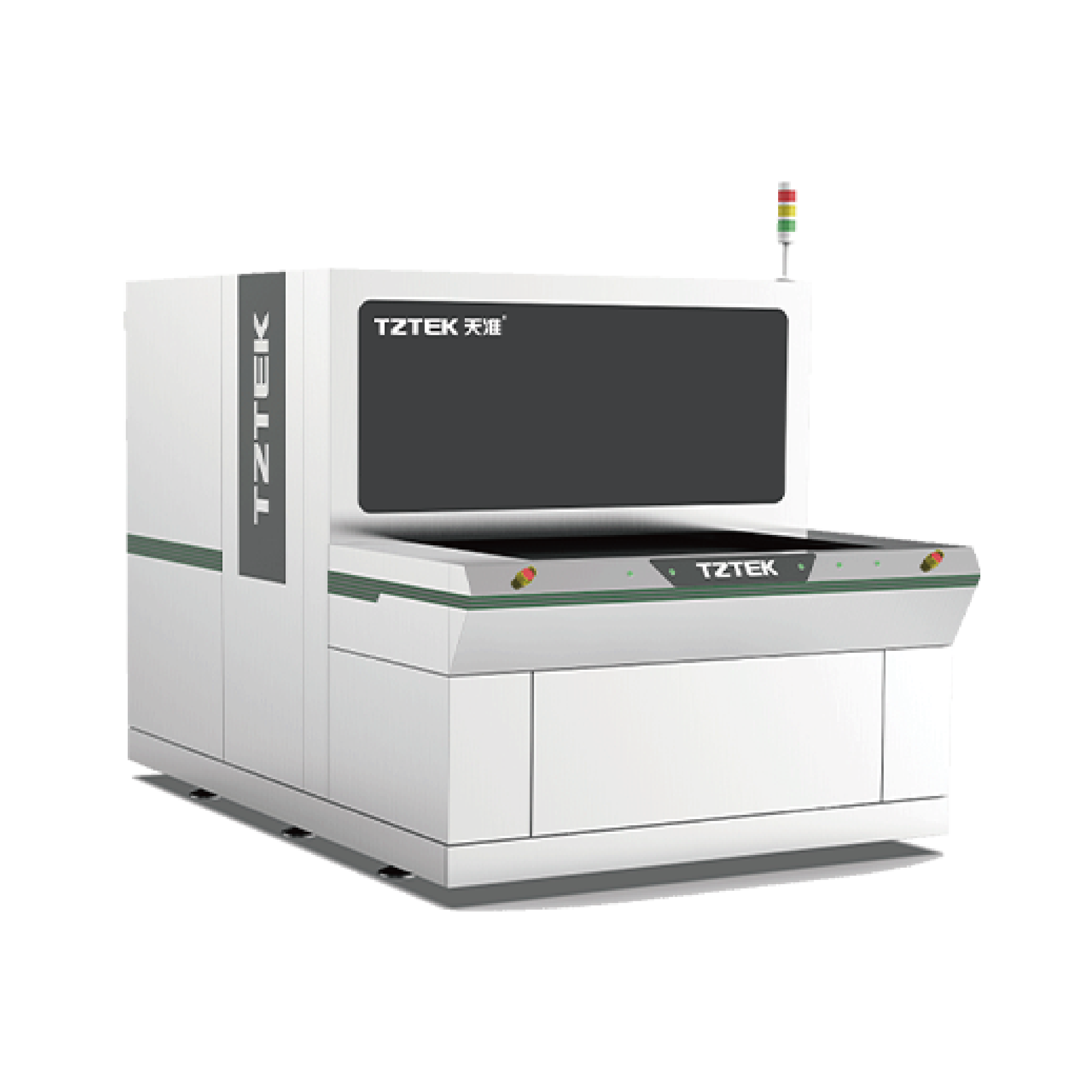
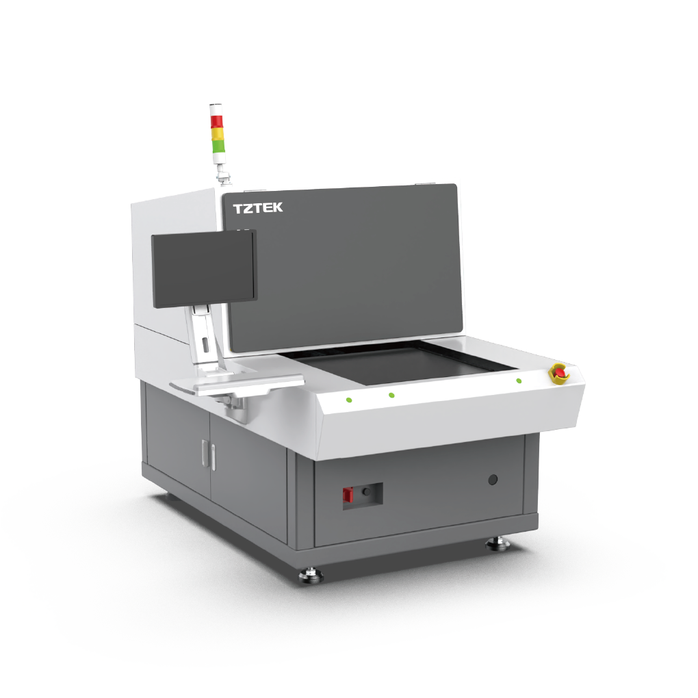
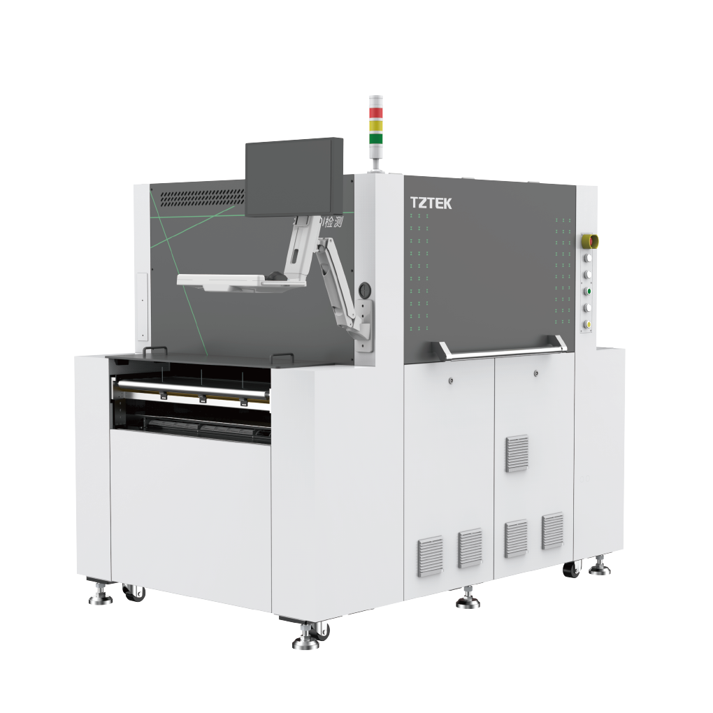
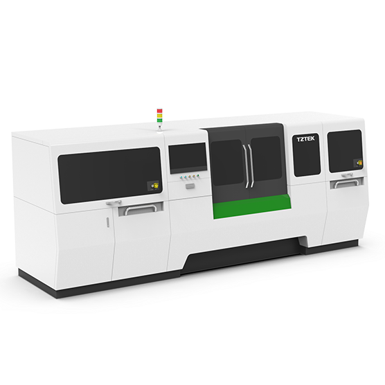
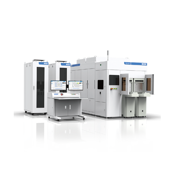
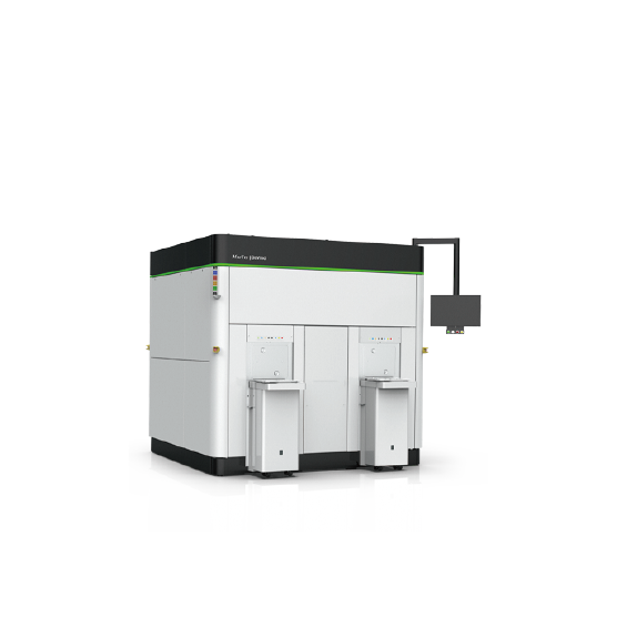
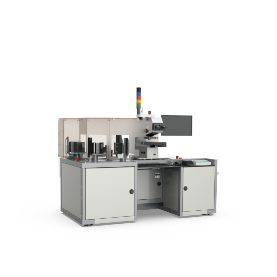
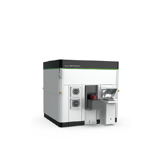
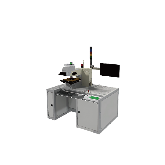
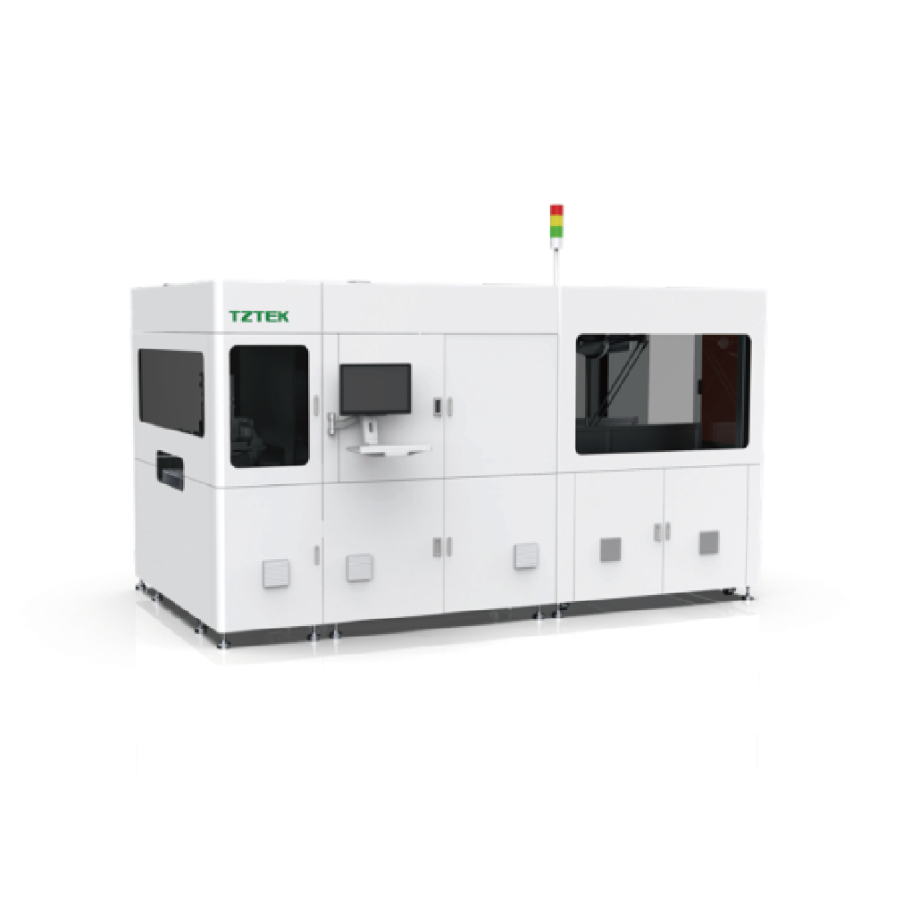
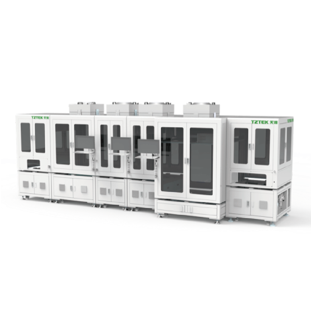
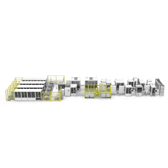
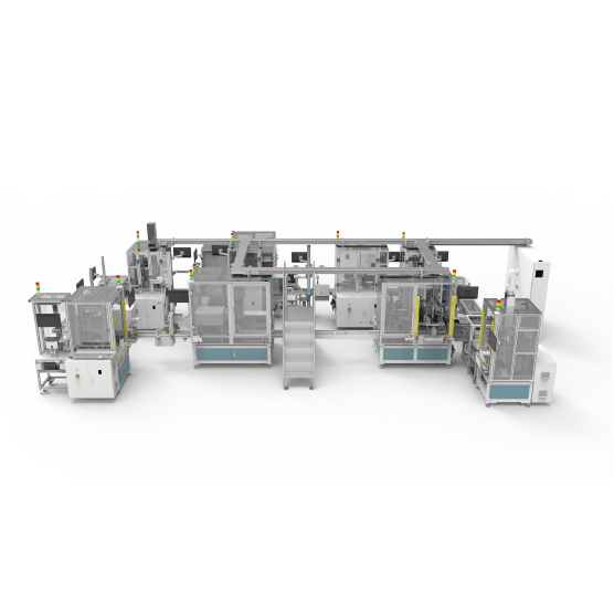
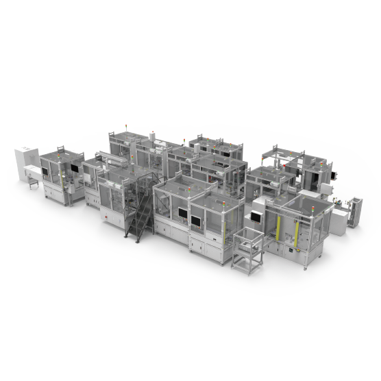
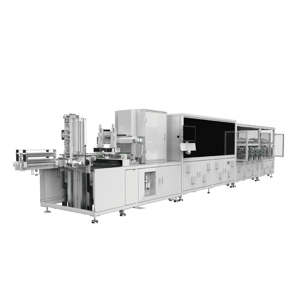


Darkfield Inspection

INDUSTRY SOLUTION
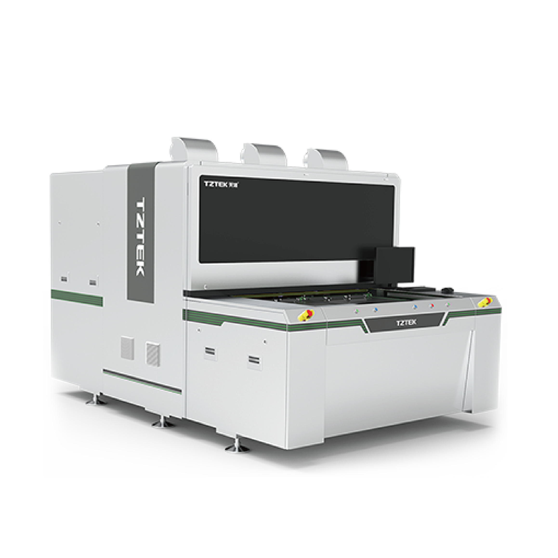
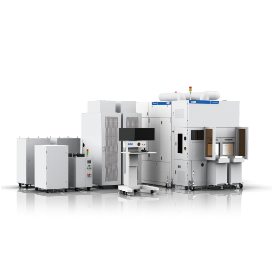
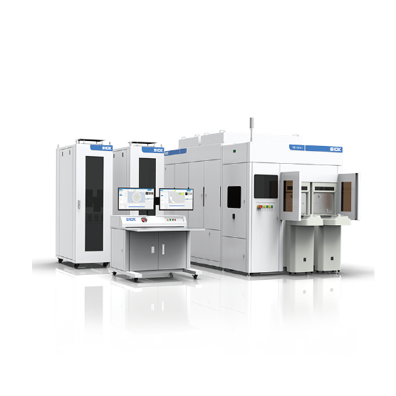
Supports a 266 nm inspection wavelength to significantly improve sensitivity to small defects.
GDS-based ROI definition improves ROI accuracy, enhances defect SNR, and suppresses noise from non-critical areas.
Advanced AI algorithms further optimize defect signal analysis.
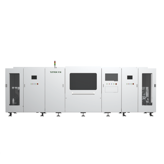
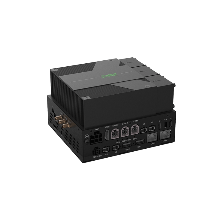
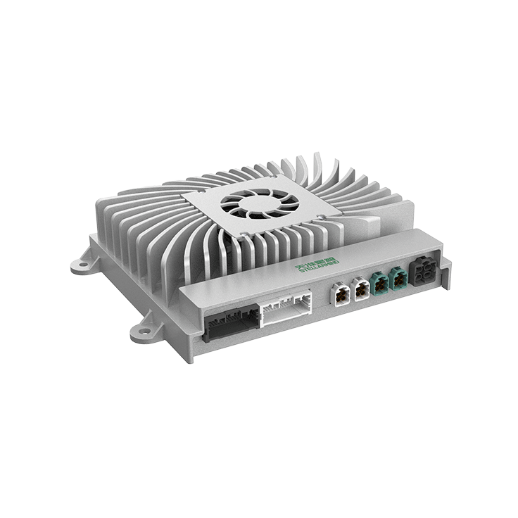
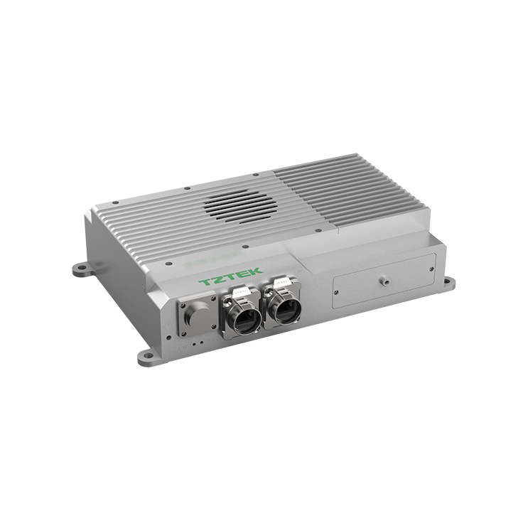
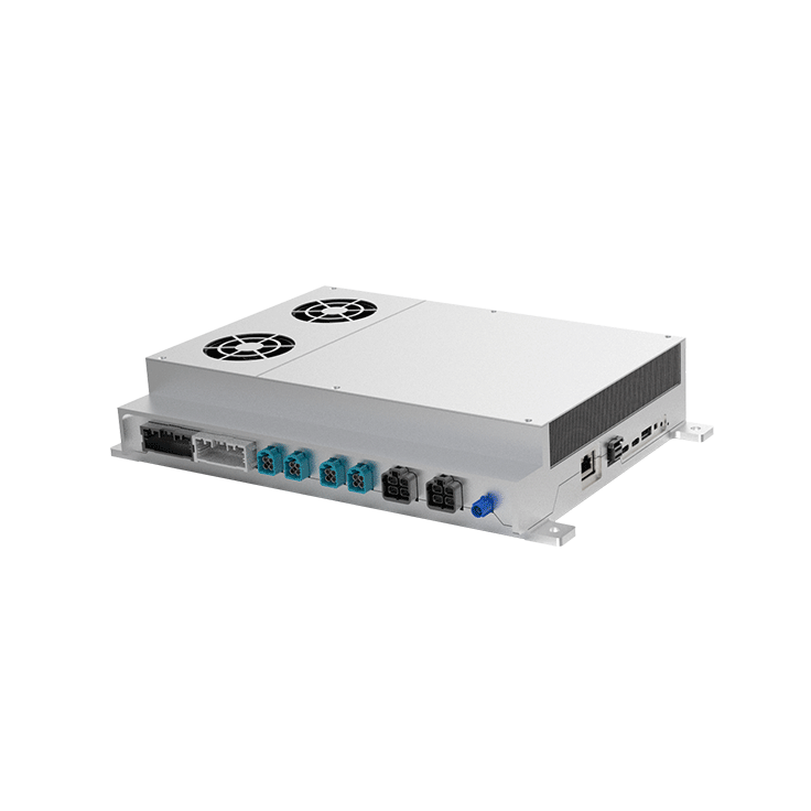
Combines a high-speed motion stage with HPC to accelerate wafer handling and data processing, increasing overall WPH throughput for high-volume manufacturing.
KEY ADVANTAGES
-


GDS ROI Technology: Higher ROI accuracy with lower inspection noise.
-

AI Algorithms & Data Analytics: Intelligent inspection, noise suppression, and support for diverse applications.
-

High-Speed Motion stage: Faster motion improves overall inspection throughput.