






























Sputtering Target Flatness Measurement
INDUSTRY CHALLENGES
-
 01
01Conventional contact profilometers and CMMs rely on point-by-point scanning, resulting in long measurement times.
-
02
Contact probes can scratch or deform the target surface, potentially affecting service life and sputtering performance.
-
03
Contact measurement can introduce contamination and compromise yield.


INDUSTRY SOLUTION
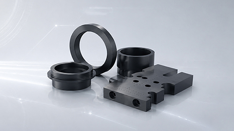
Magnetron sputtering, a widely used PVD process, deposits conductive, dielectric, and protective films onto substrates. Target flatness is critical to ensuring uniform, dense film deposition, as well as maintaining purity and thermal conductivity.
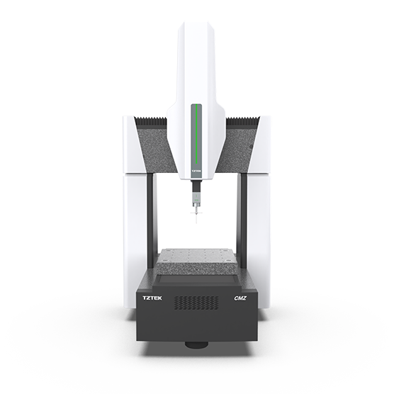
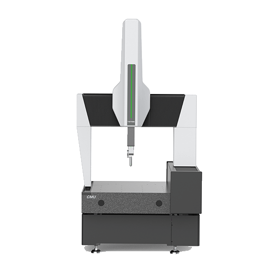
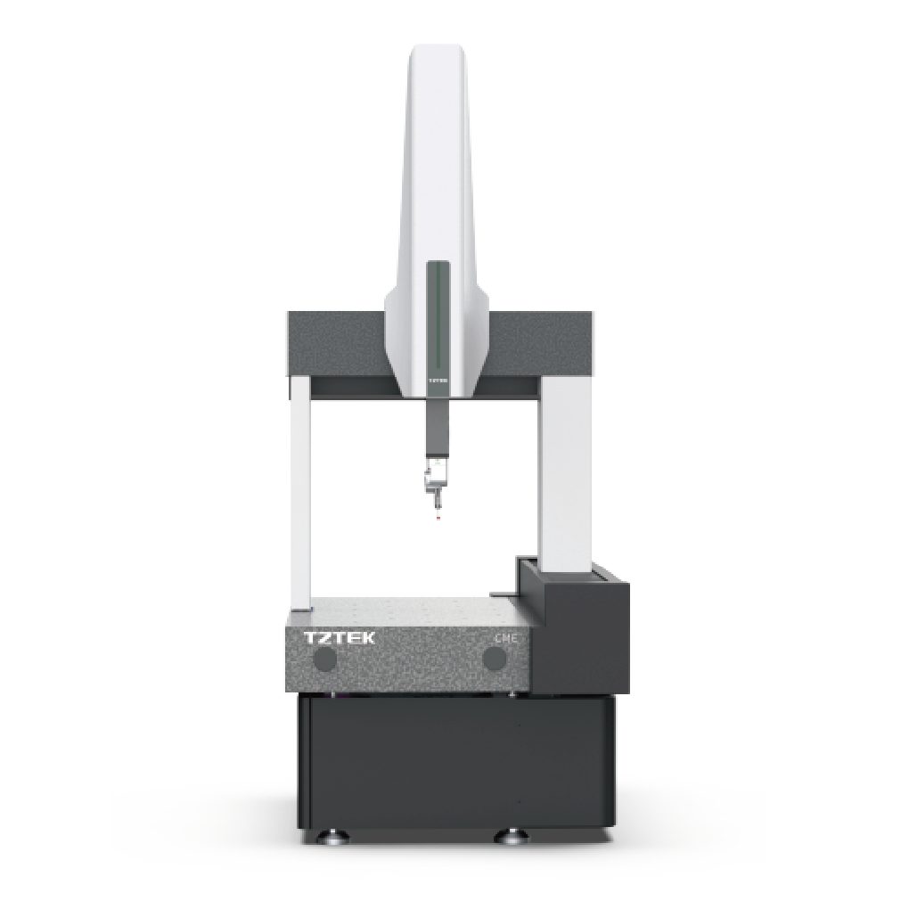
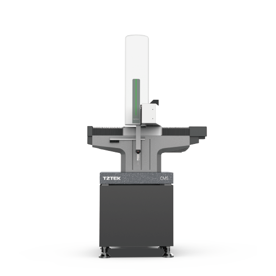
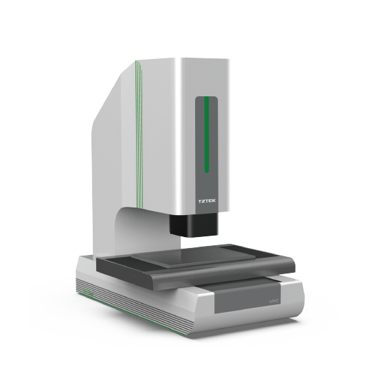
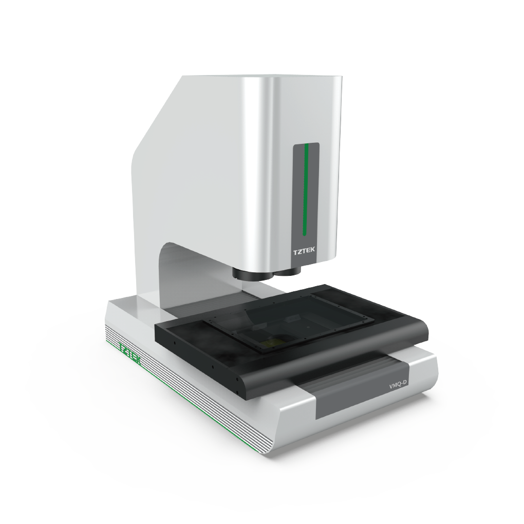
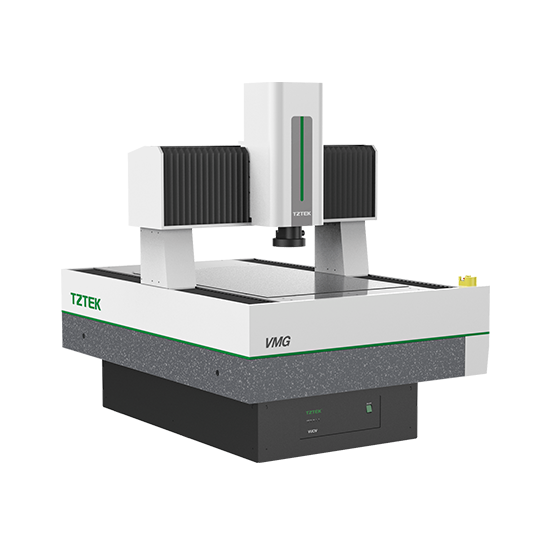
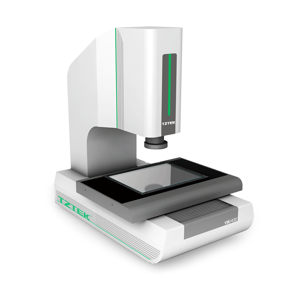
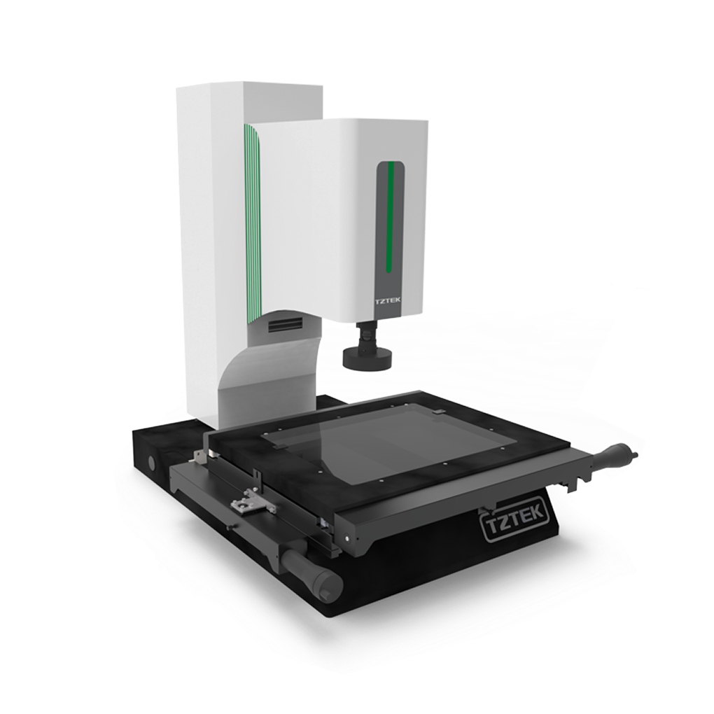
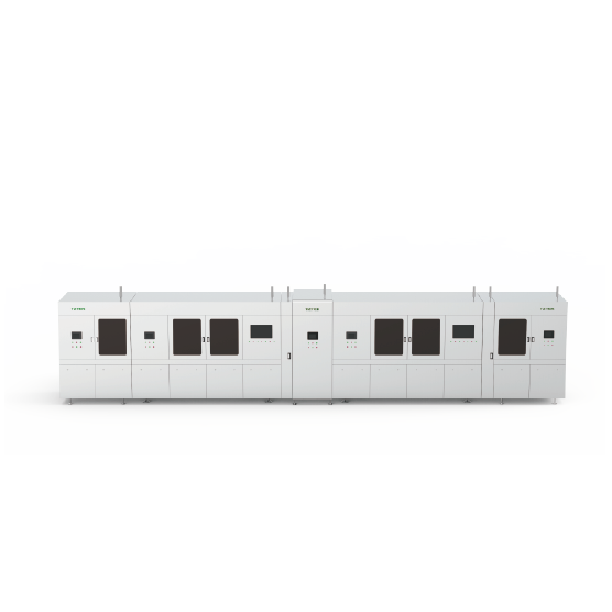
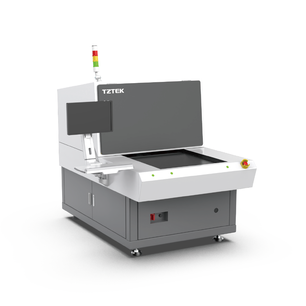
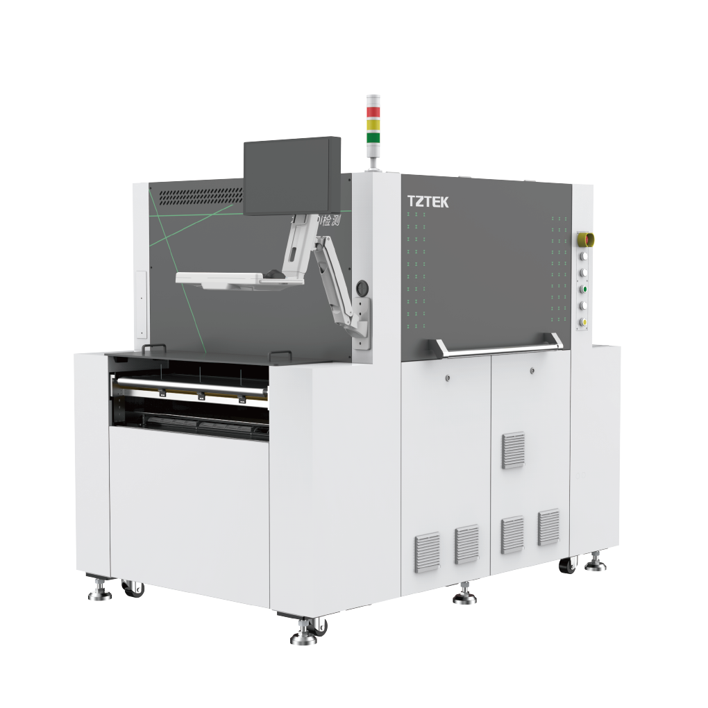
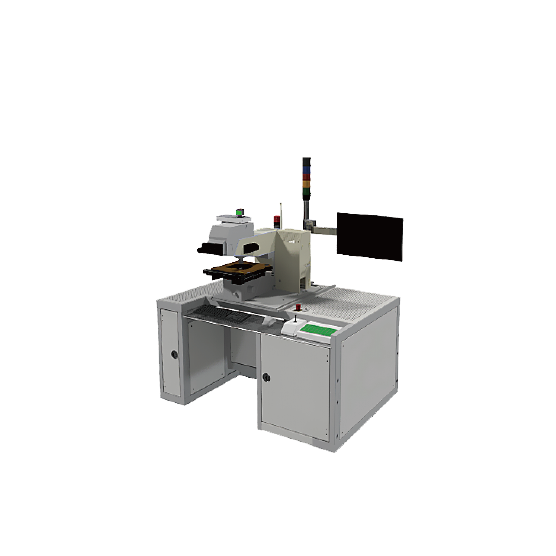
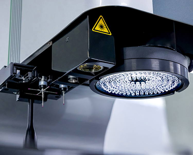
TZTEK’s vision measuring system integrates a spectral confocal sensor for high-precision flatness measurement of sputtering targets.
The non-contact optical approach eliminates surface damage and contamination risks while enabling high-speed inspection for high-volume production.
KEY ADVANTAGES
-


Non-contact measurement eliminates surface damage and contamination risks.
-

Flexible configuration with multiple spectral confocal sensor options to meet different accuracy requirements.
-

Supports both single-point and scanning modes.