




MEMS & Bonding Process Control
INDUSTRY CHALLENGES
-
 01
01Limited Visible-Light Transmission: Visible light cannot penetrate silicon, making bonding interfaces and internal structures difficult to inspect.
-
02
Challenging Bonding Void Detection: Particles and contamination can cause bonding voids that compromise sealing and reliability, requiring non-destructive inspection.
-
03
Heavily Doped Wafer Imaging: Heavily doped MEMS wafers cause significant IR attenuation, requiring optimized optics and algorithms.


INDUSTRY SOLUTION
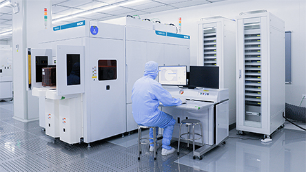
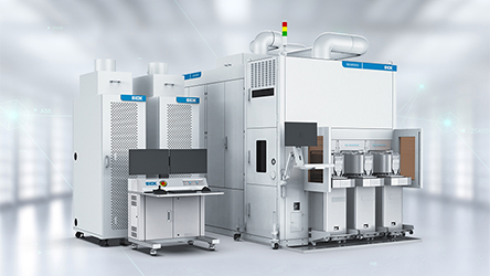
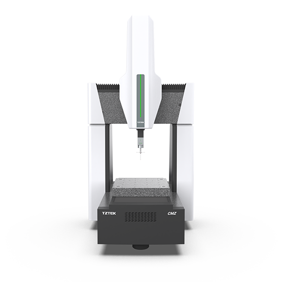
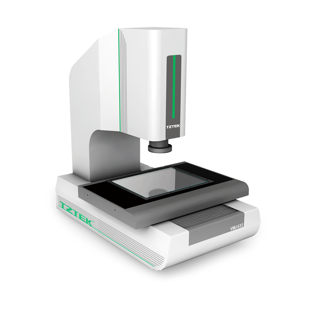
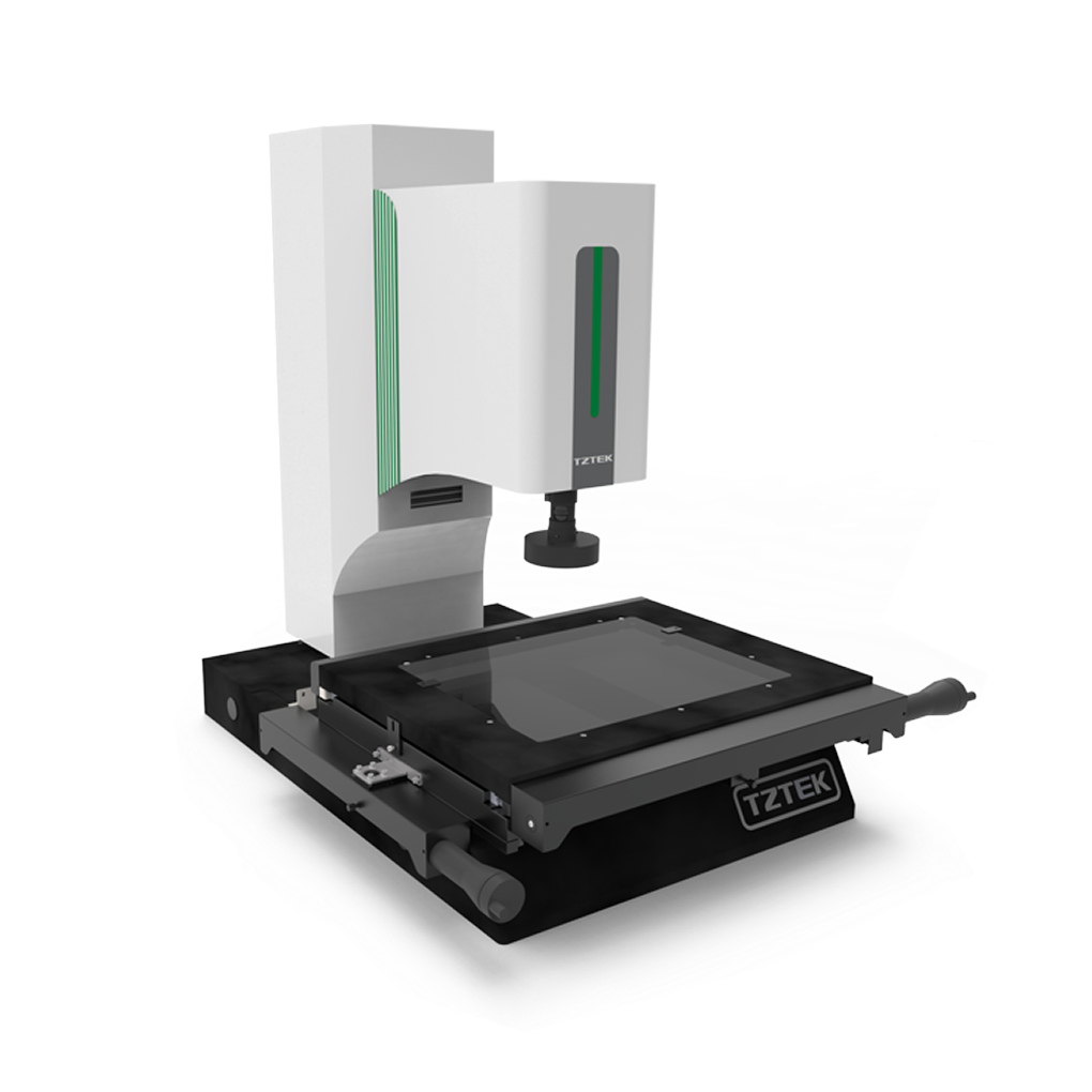
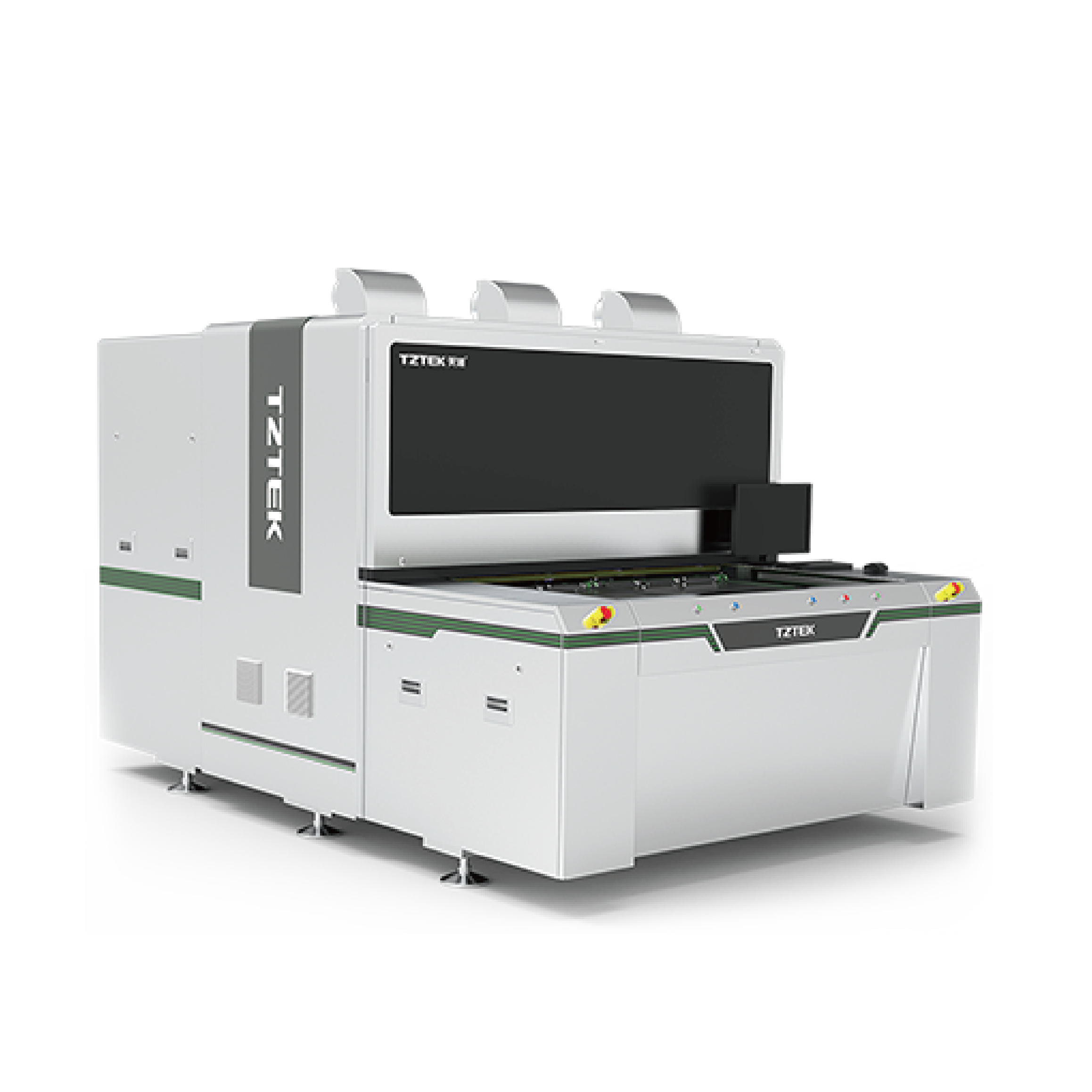
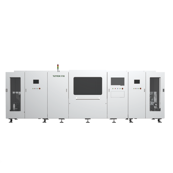
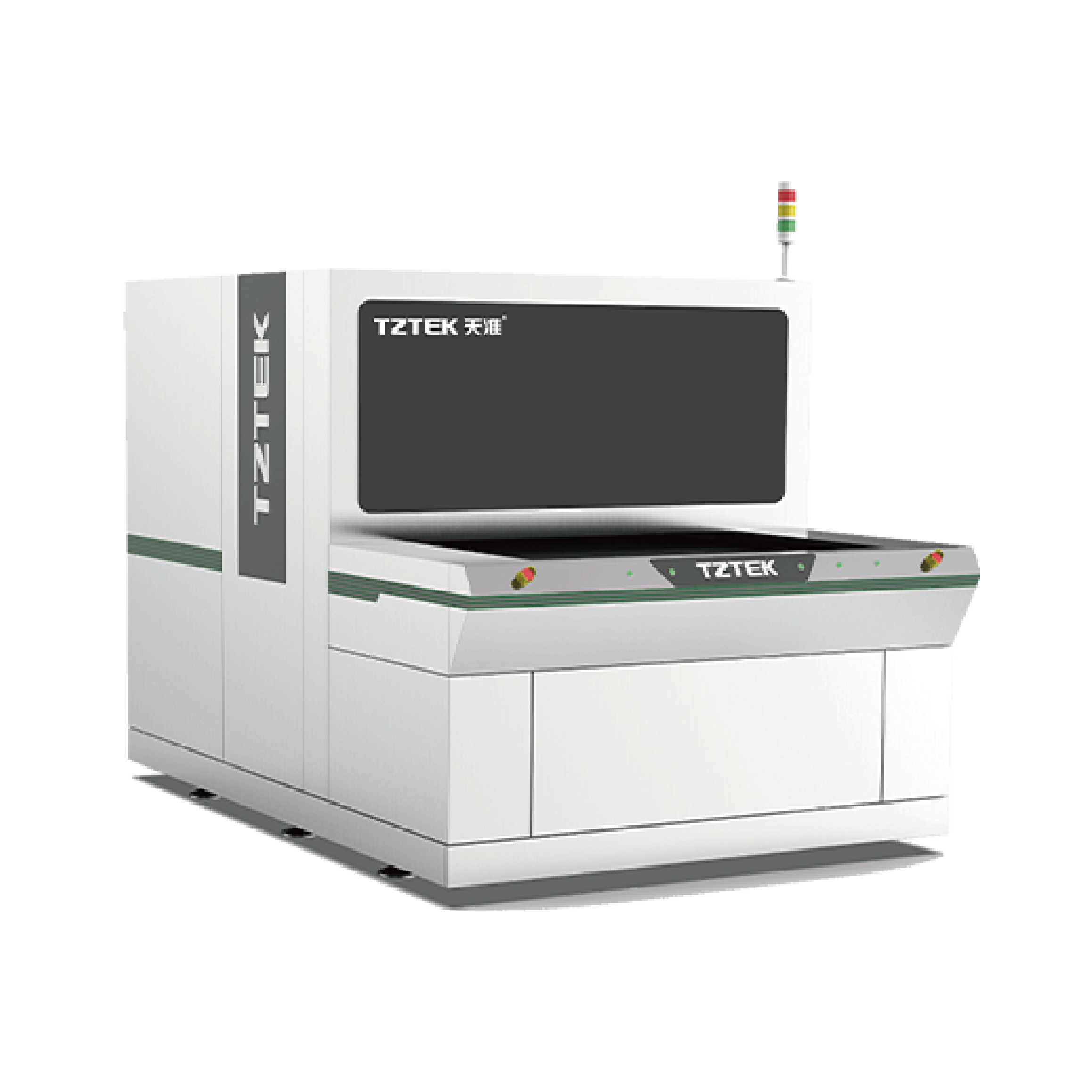
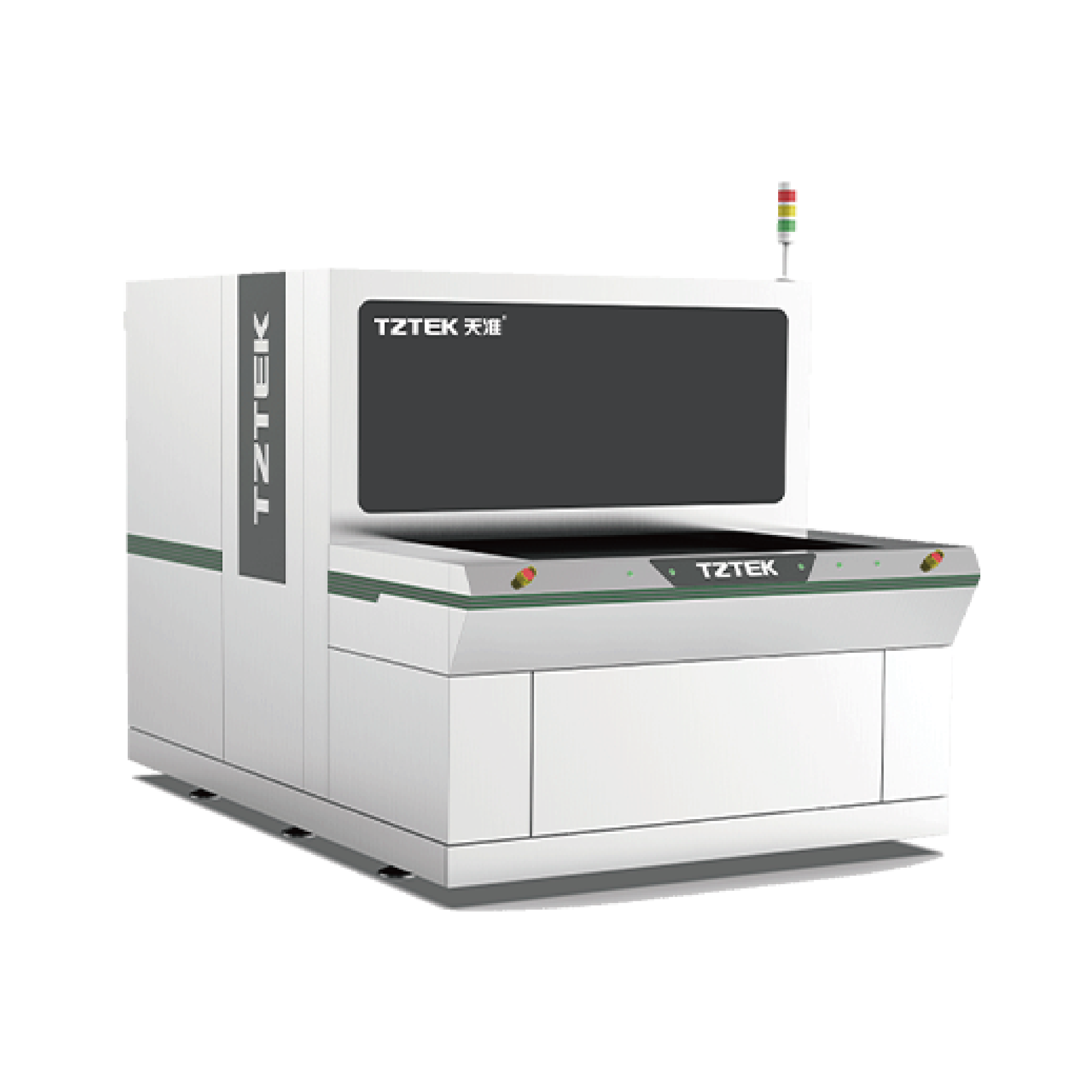
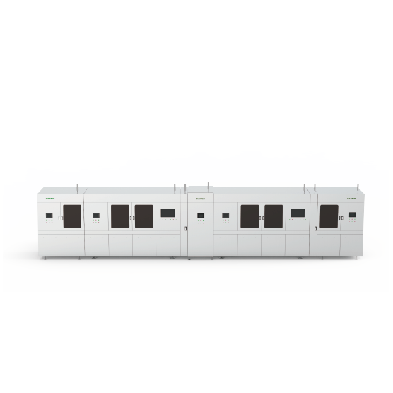
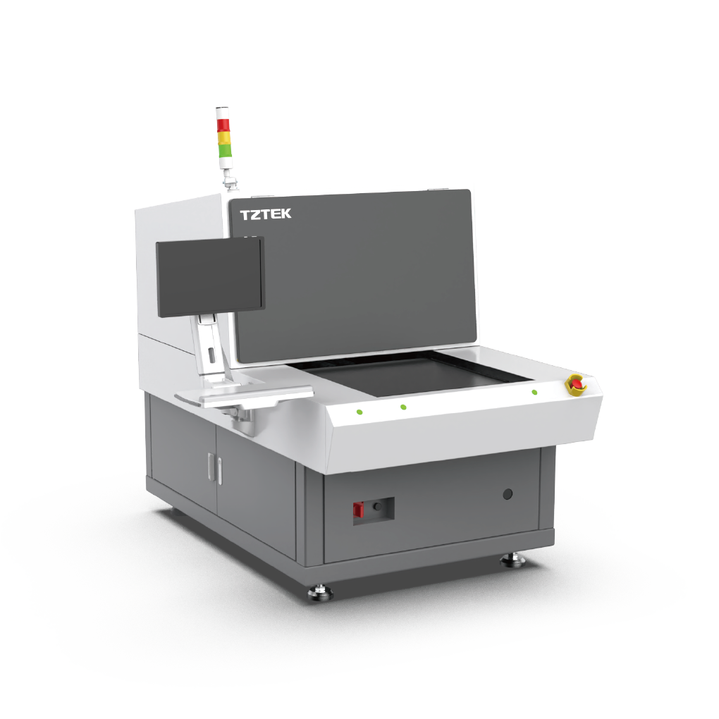
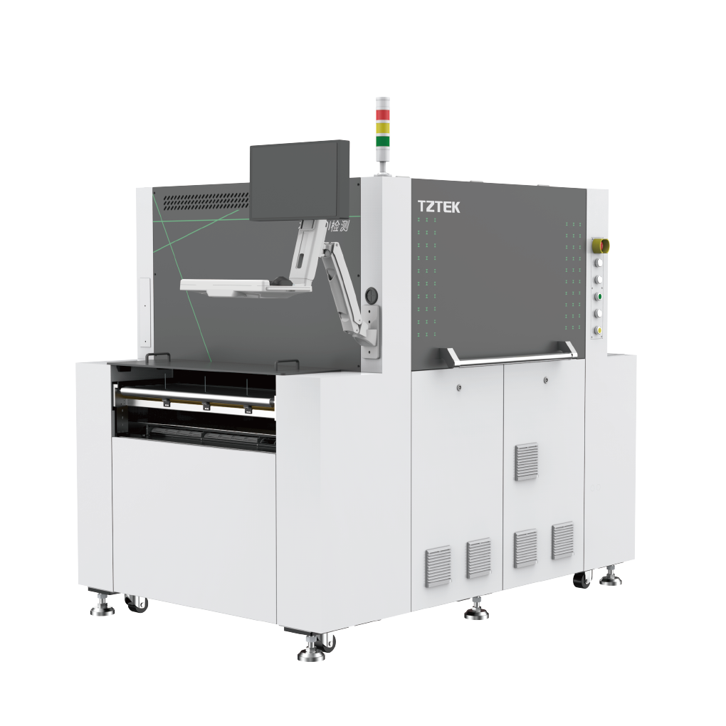
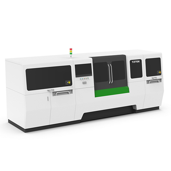
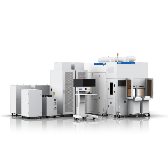
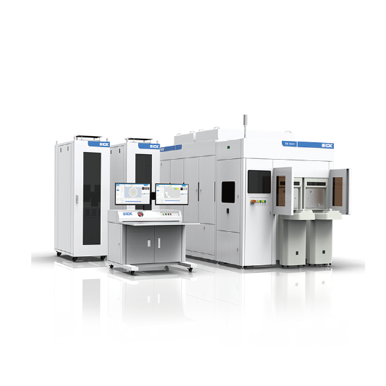
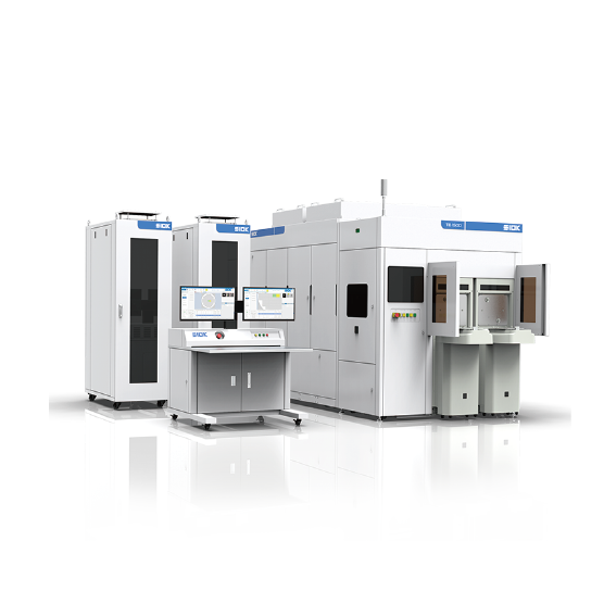
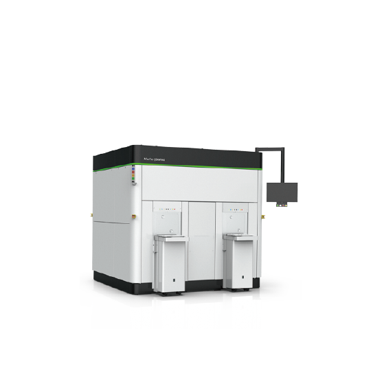
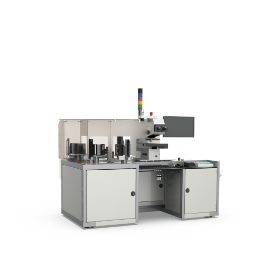
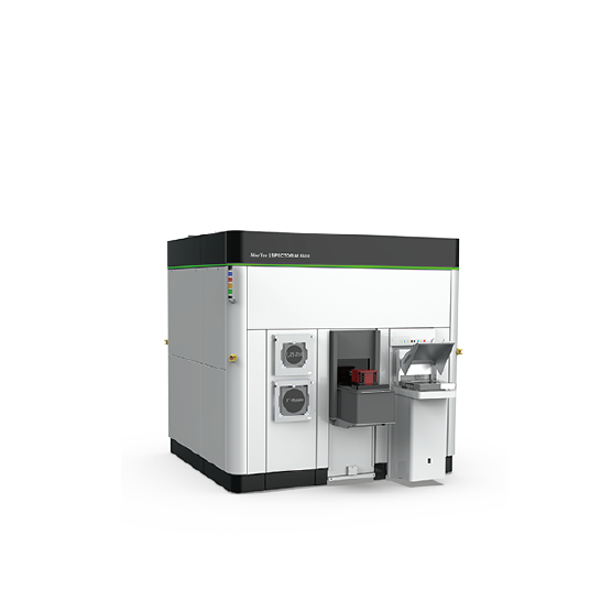
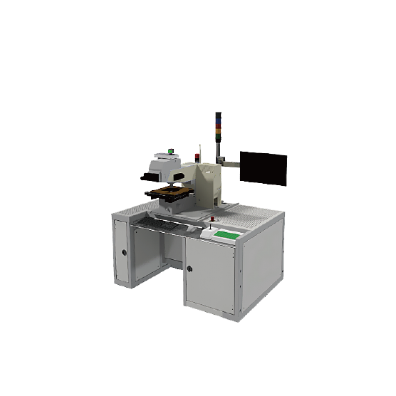
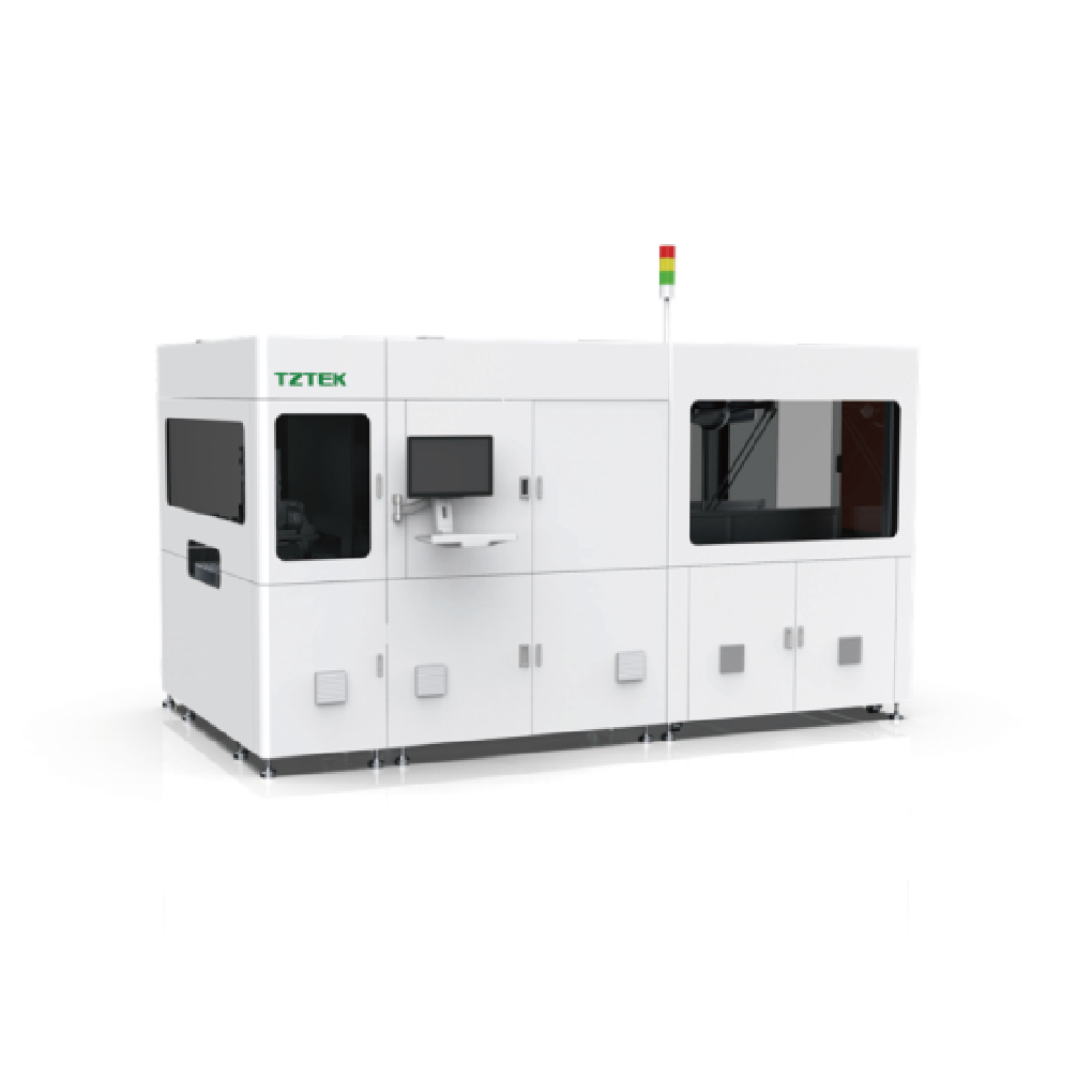
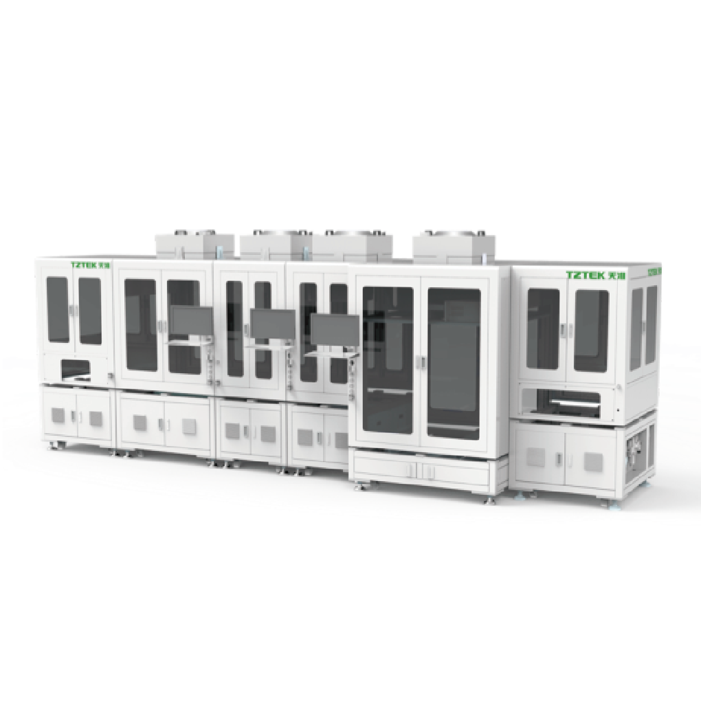
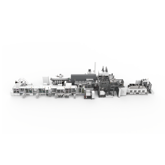
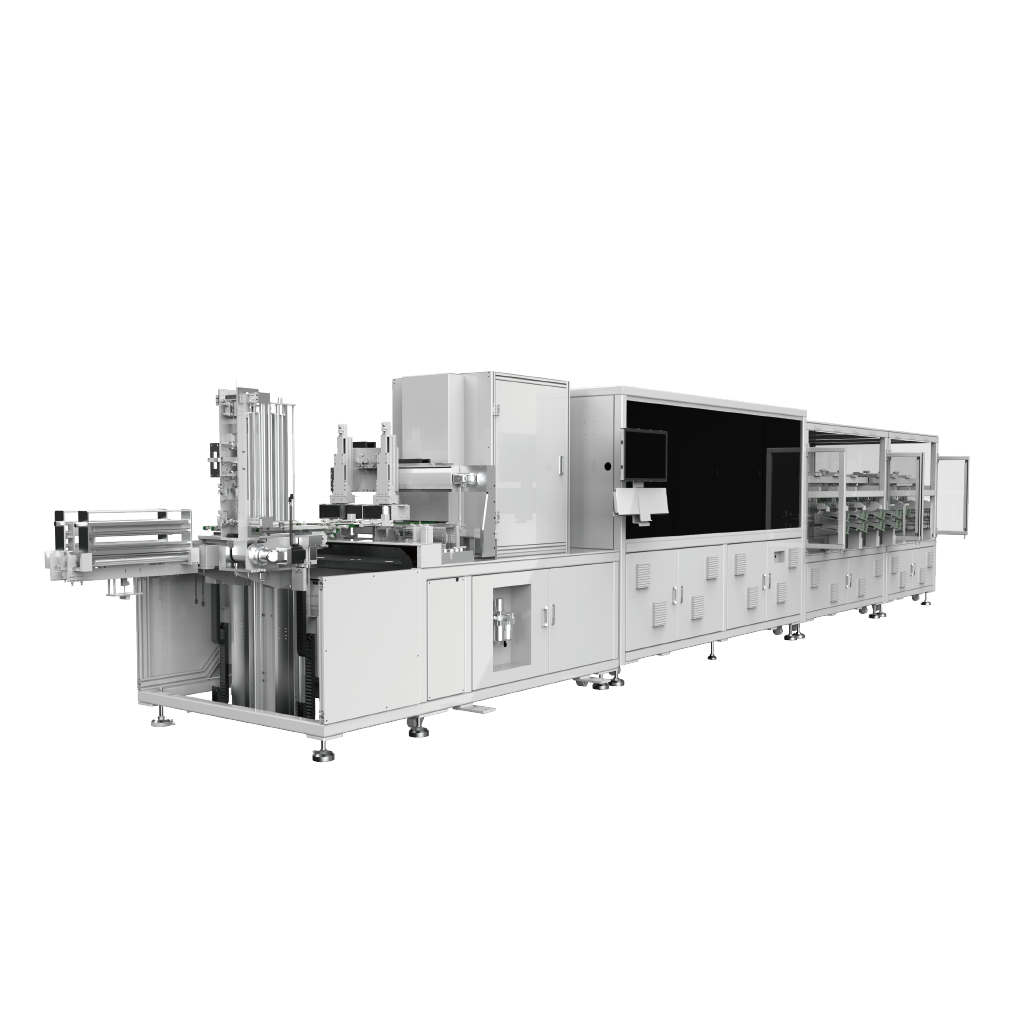
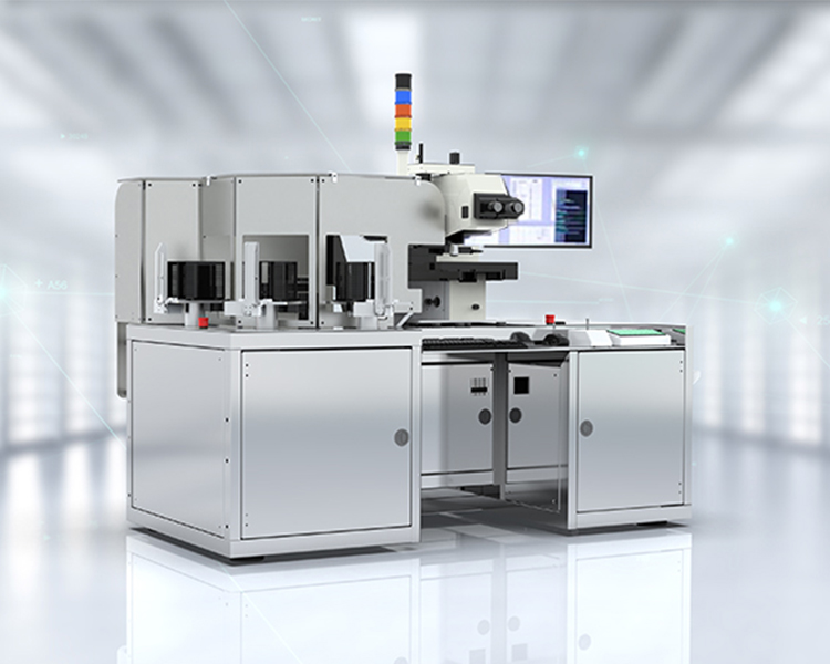
To address the non-destructive inspection and precision metrology needs of MEMS and wafer bonding processes, TZTEK provides dedicated solutions based on the DaVinci IR Series and MT IR (IRIS) Series.
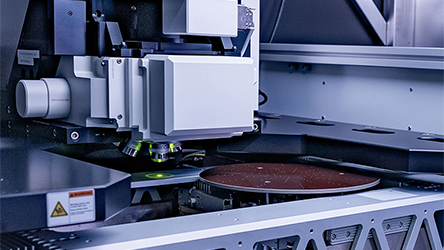
Leverages the transparency of silicon and GaAs at 1050–1550 nm with high-performance InGaAs cameras and optimized visible/IR illumination and reflection/transmission optics for non-destructive inspection through the wafer.
Detects bonding defects, voids, and cracks after eutectic and glass bonding, while supporting post-bond overlay and CD metrology on a single platform.
DaVinci 200IR/300IR supports 200 mm and 300 mm wafers, while IRIS 2100 covers wafer sizes from 75 to 200 mm. All systems support SECS/GEM communication for intelligent process control in MEMS and wafer bonding R&D and high-volume manufacturing.
KEY ADVANTAGES
-


Through-Wafer IR Inspection: 1050–1550 nm IR imaging enables non-destructive inspection through silicon.
-

Integrated Inspection & Metrology: Bonding defects, voids, overlay, and CD measurement on a single platform.
-

Proprietary Dual-Mode Illumination: Combined visible and IR illumination distinguishes surface defects from subsurface defects.