


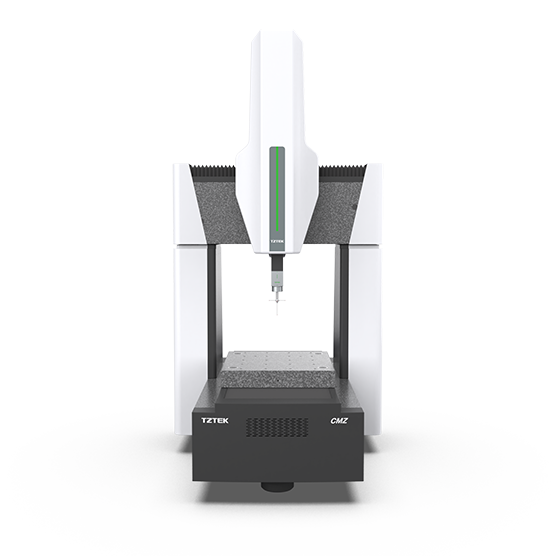
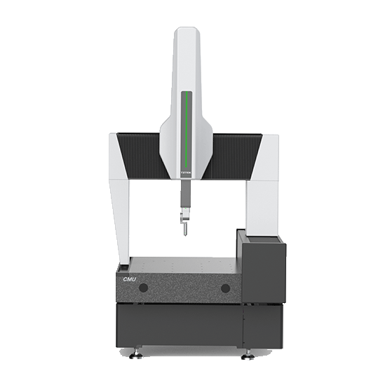
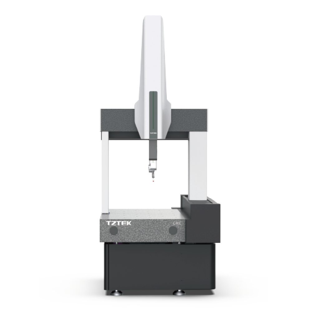
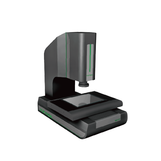
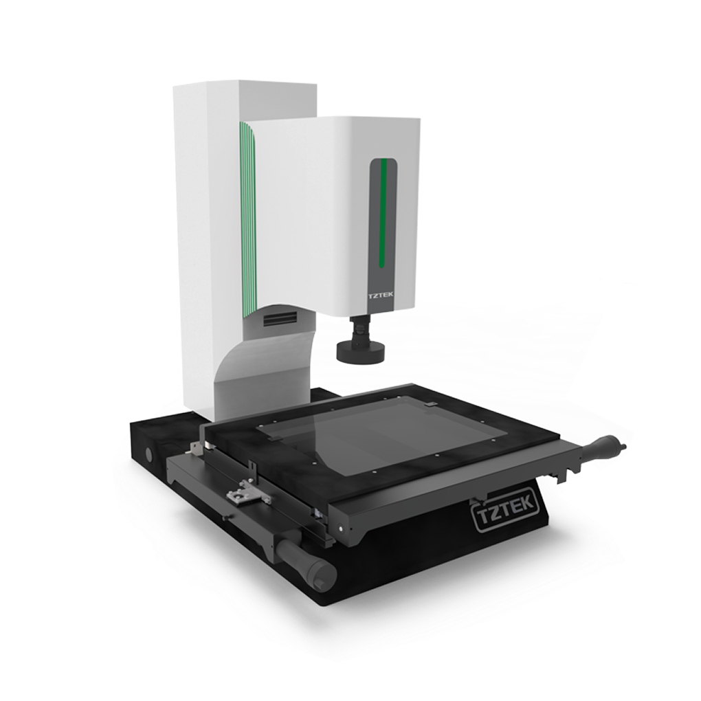
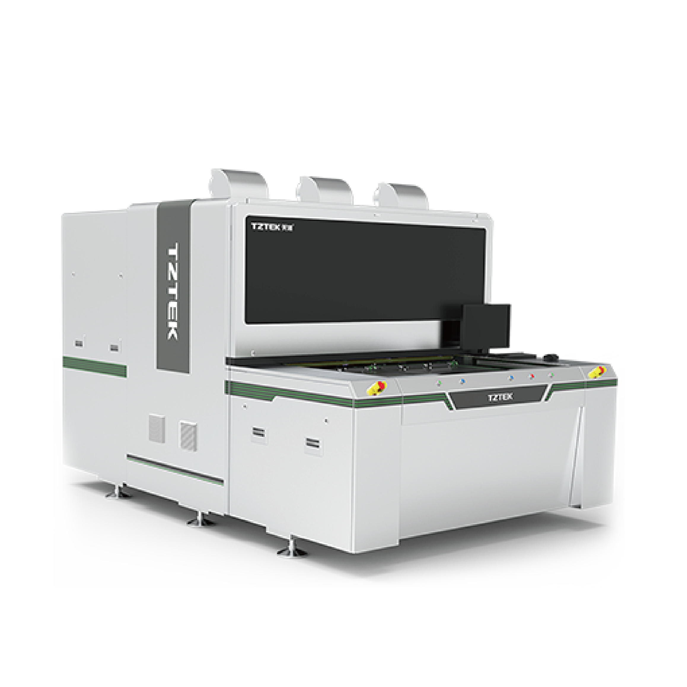
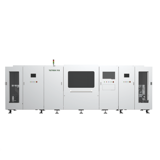
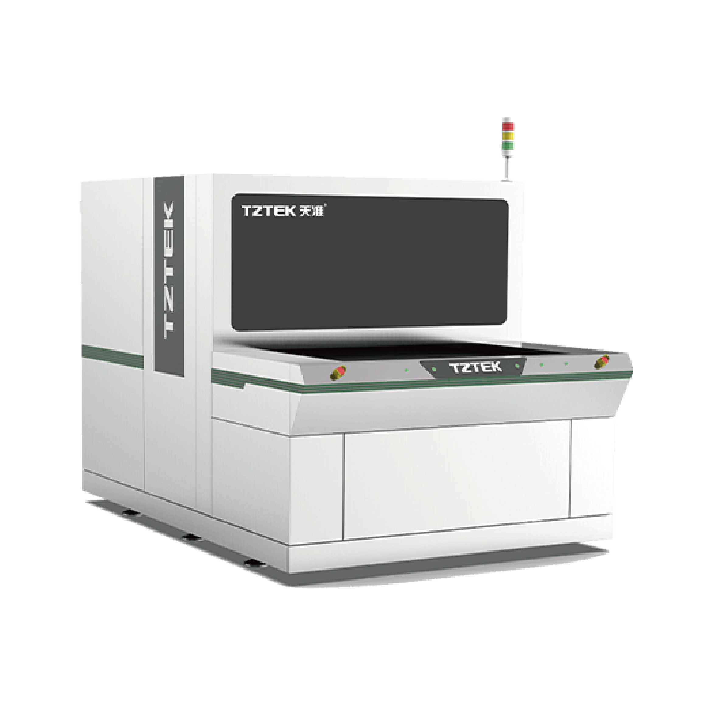
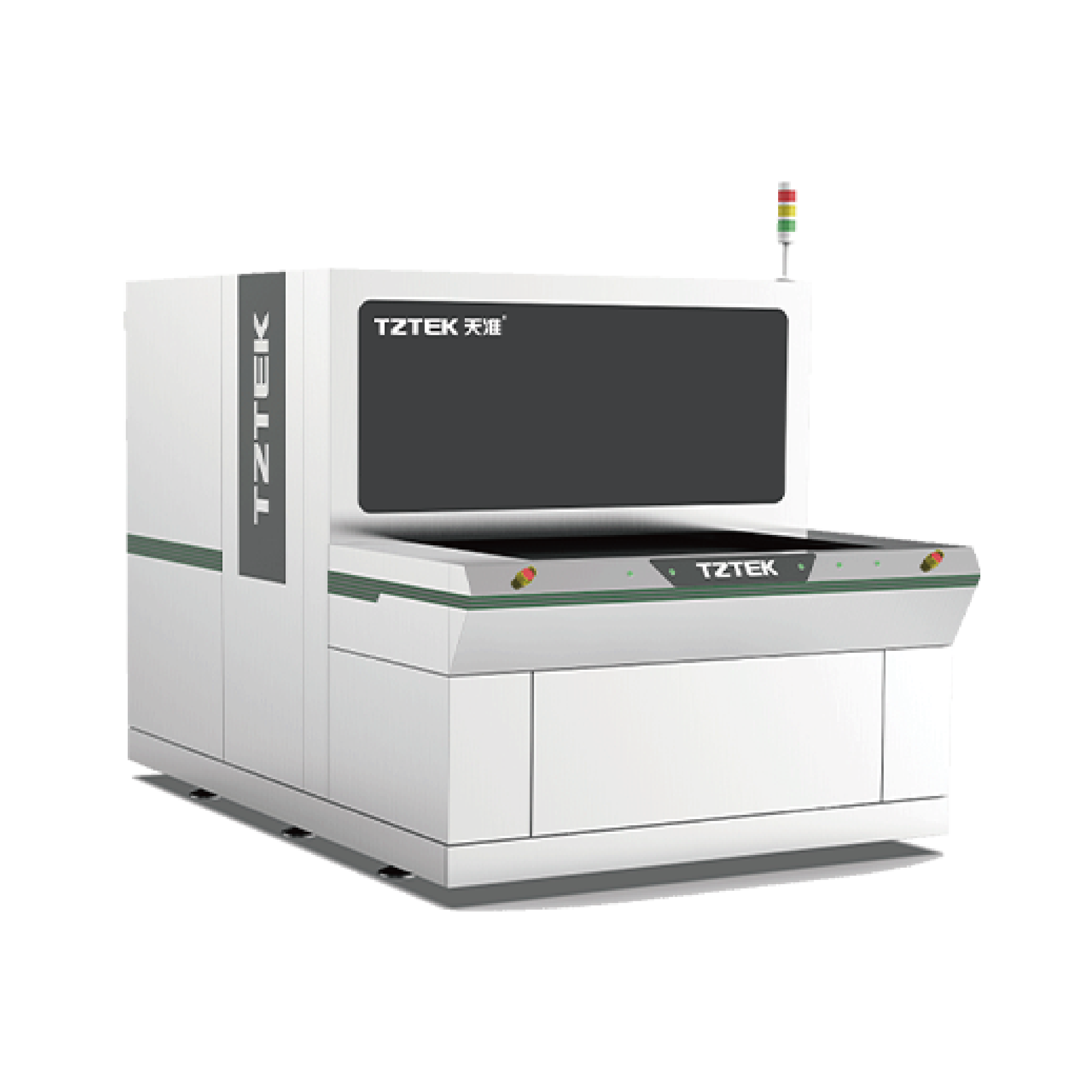
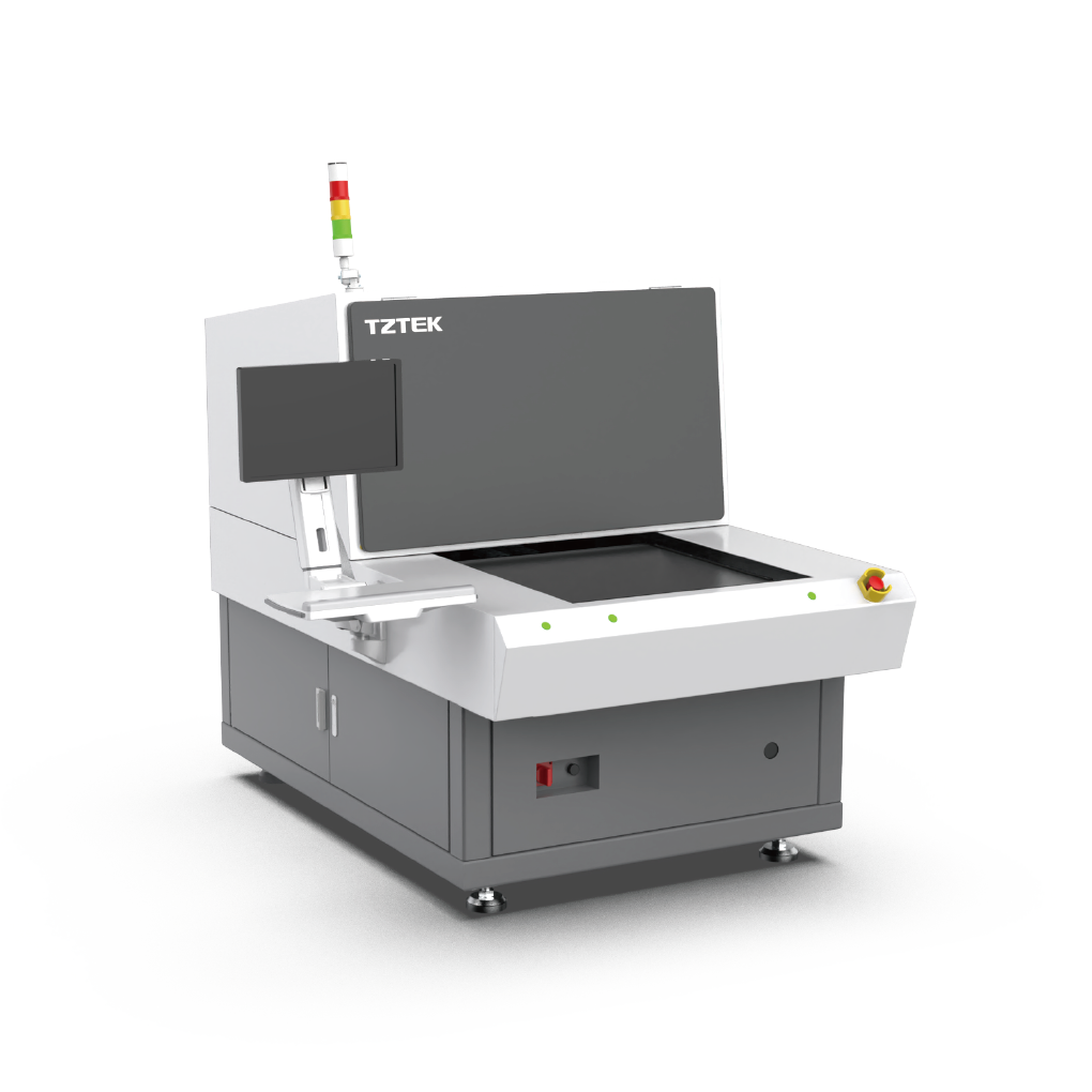
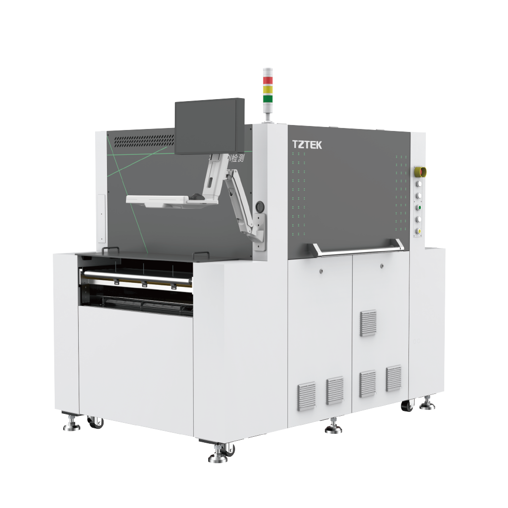
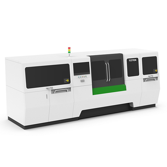
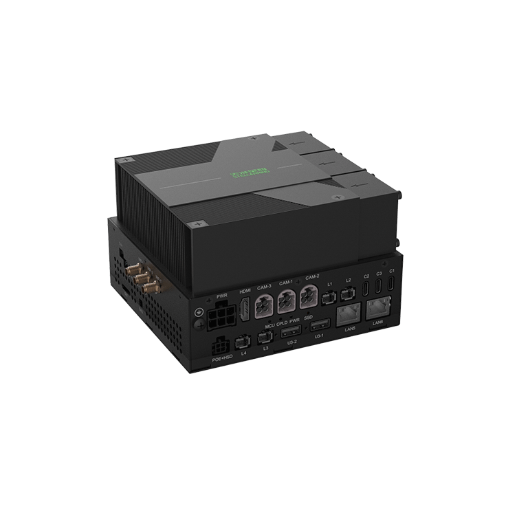
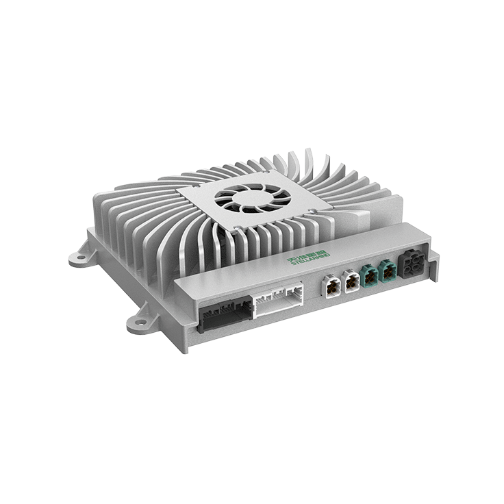
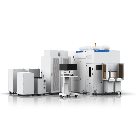
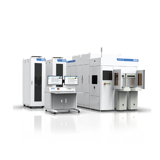
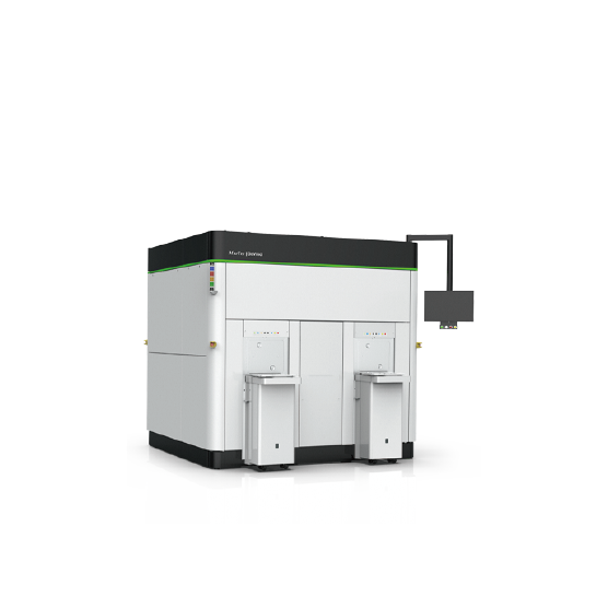
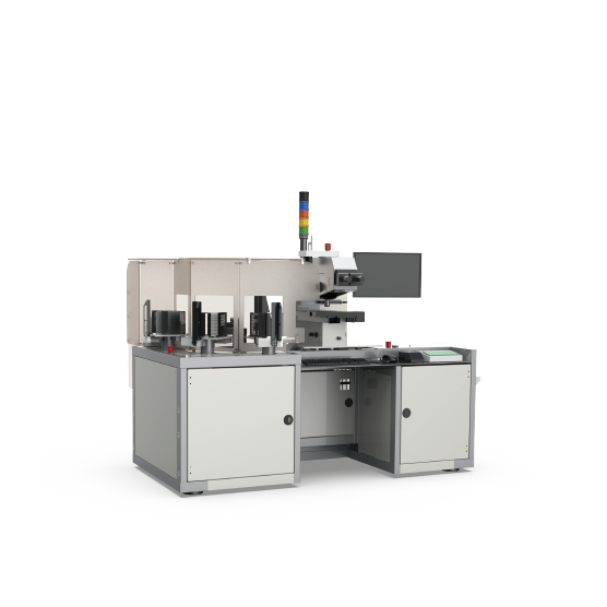
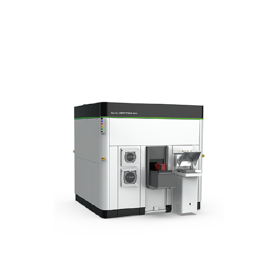
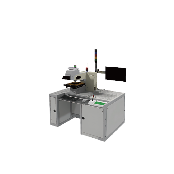
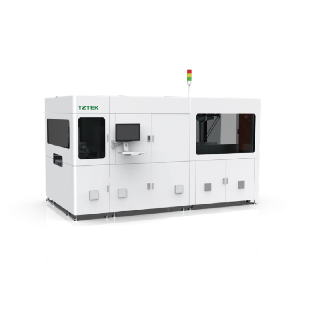
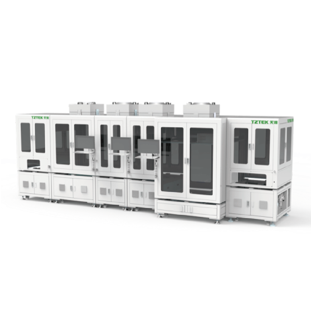
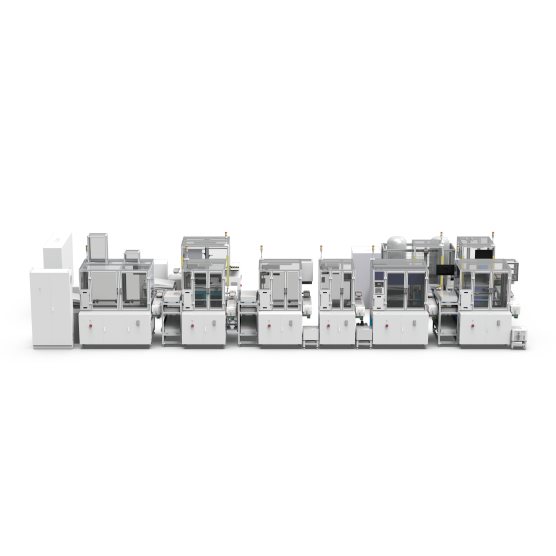
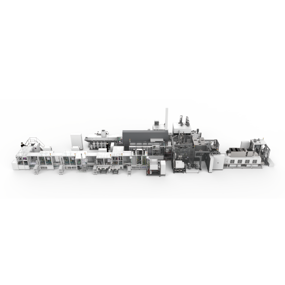
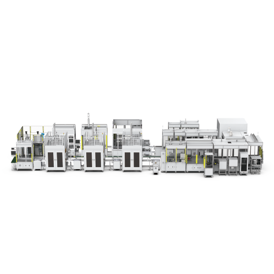
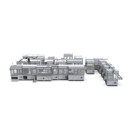
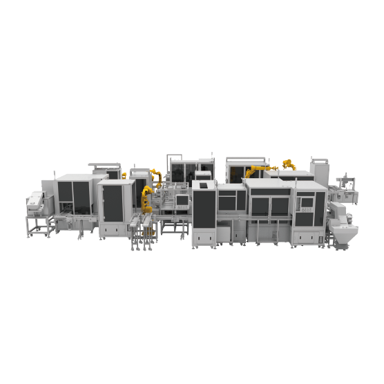
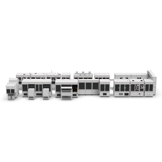
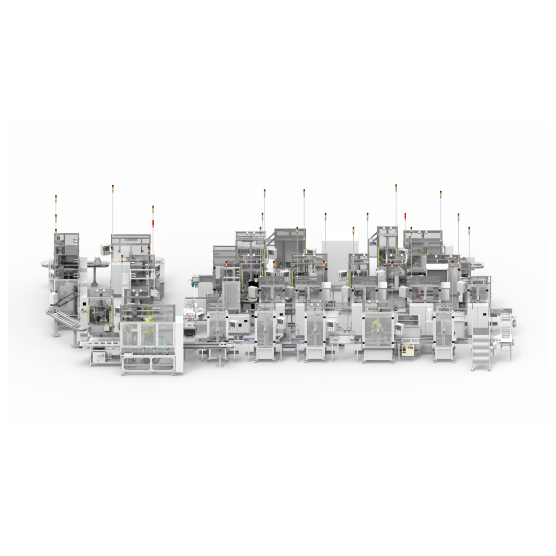
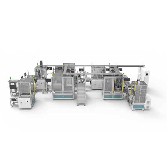
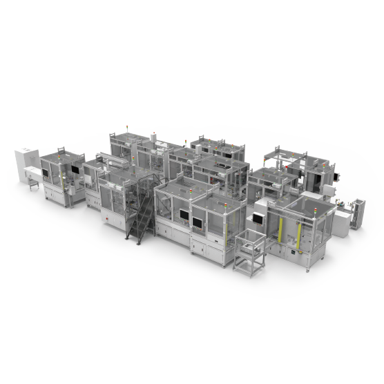
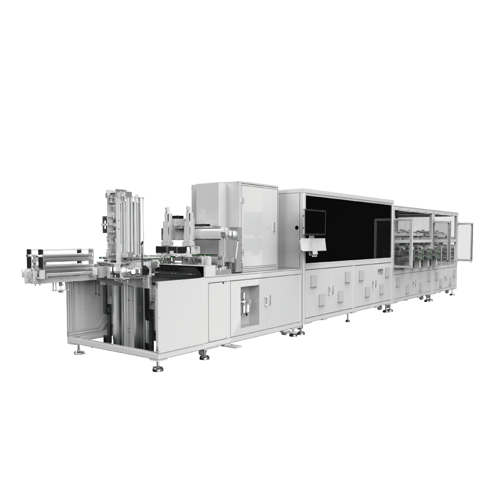


TB1100
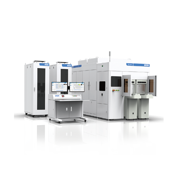
For 180-65 nm technology nodes
Compatible with 8-inch/12-inch wafers
Compatible with 8-inch/12-inch wafers
Scroll to explore
Advantages
-
High Sensitivity
-
High Throughput
-
Intelligent Software Support
-
 High Sensitivity
Defect detection down to 70 nm
Advanced signal processing for enhanced signal-to-noise ratio
Broadband illumination for comprehensive defect capture

-
 High Throughput
High data rate
Multiple pixel size options
Optimized for high-speed scanning
-
 Intelligent Software Support
Online Smart Defect Classification (SDA)
Process Window Verification