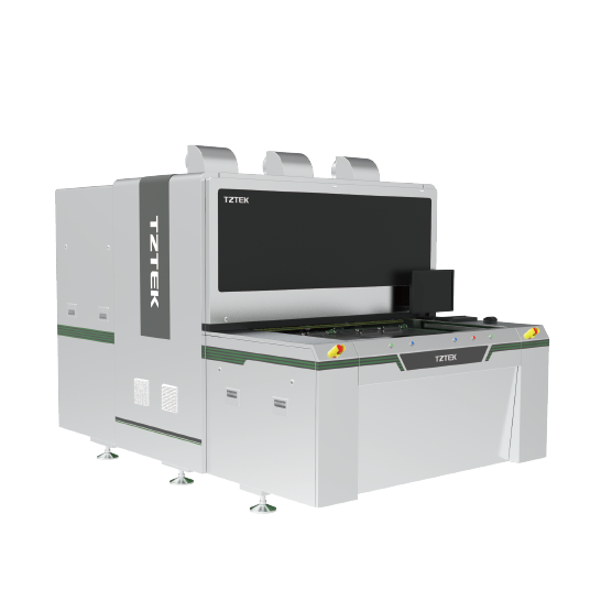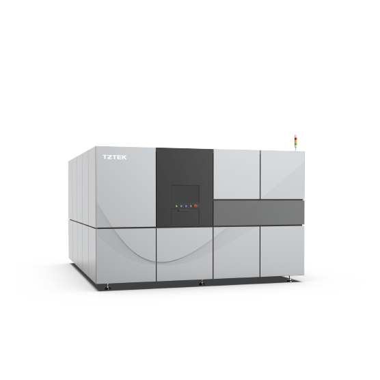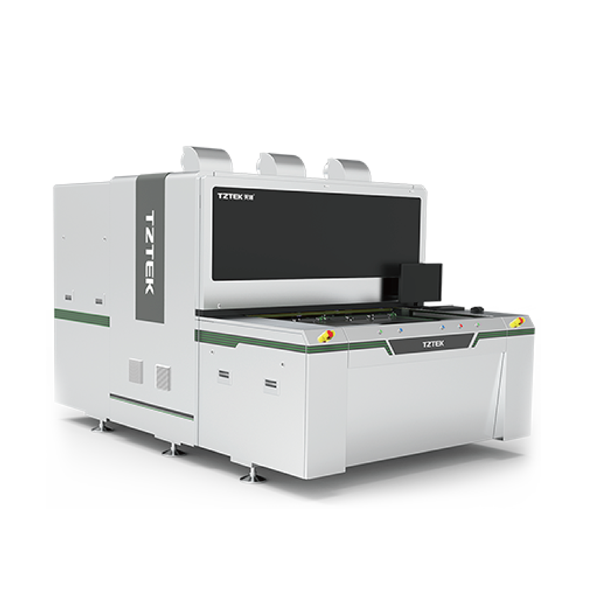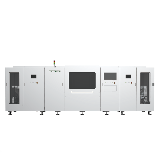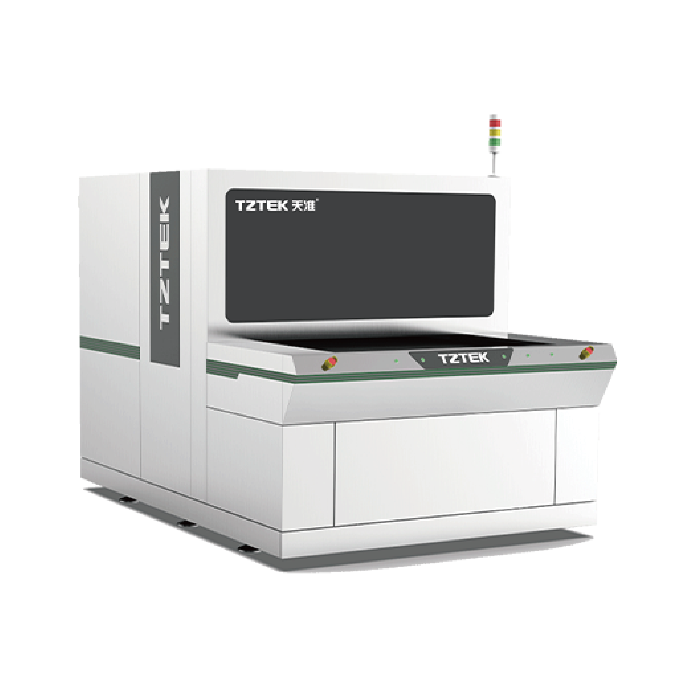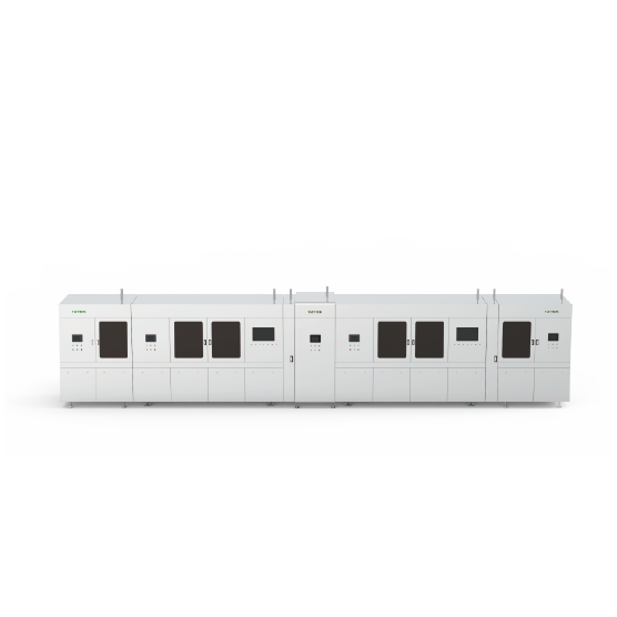



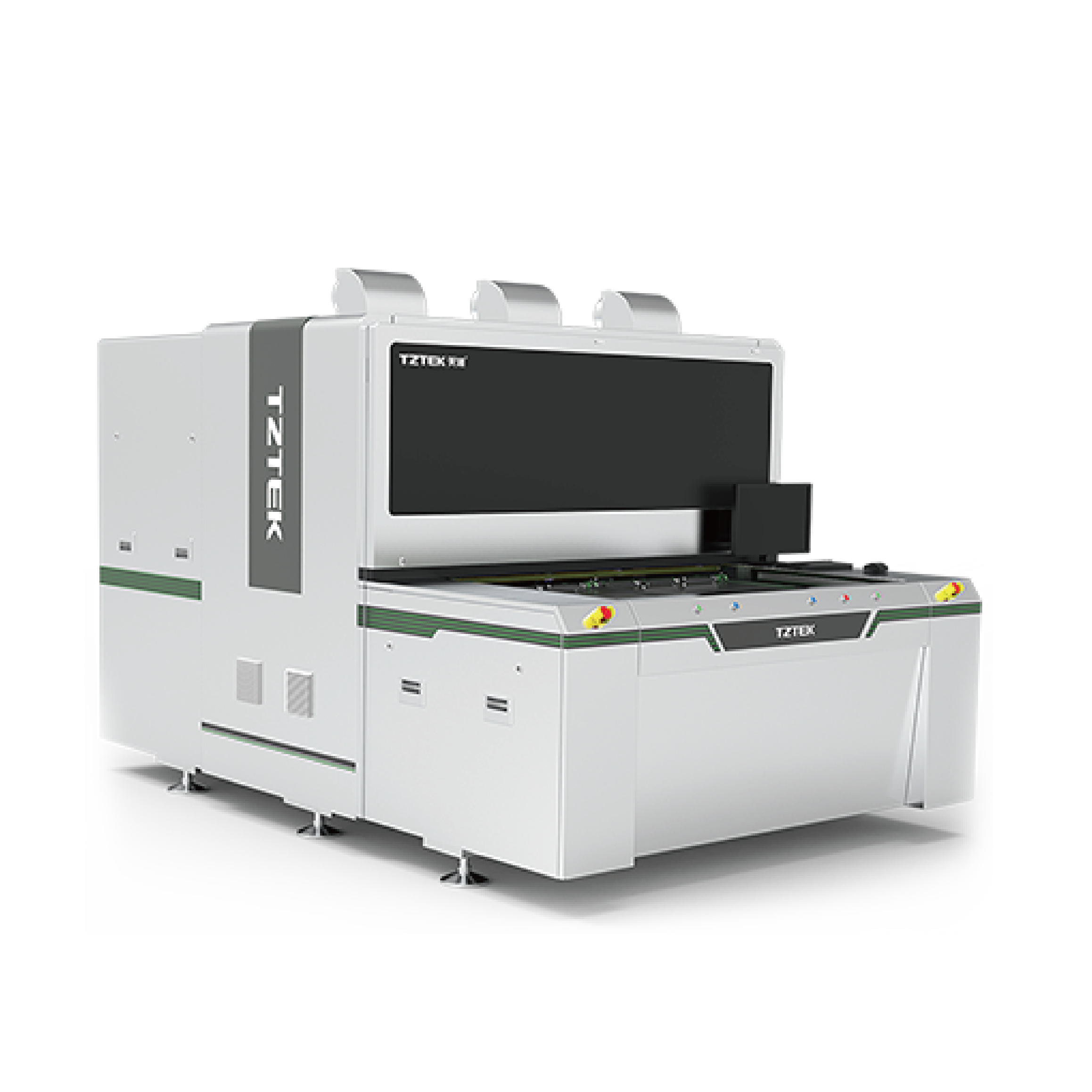
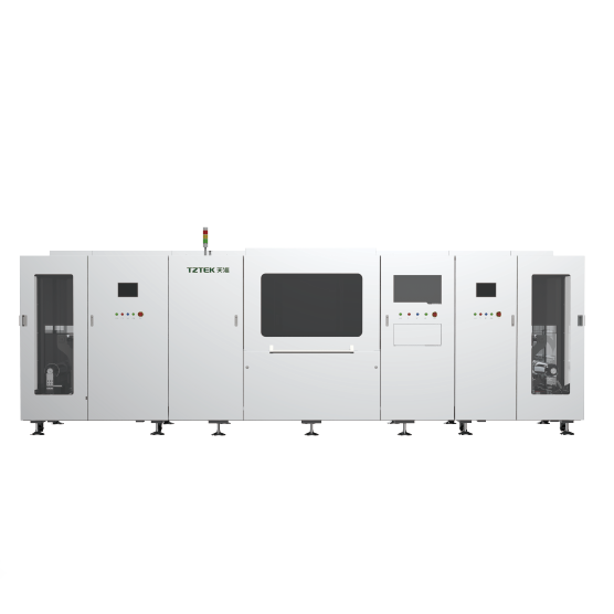
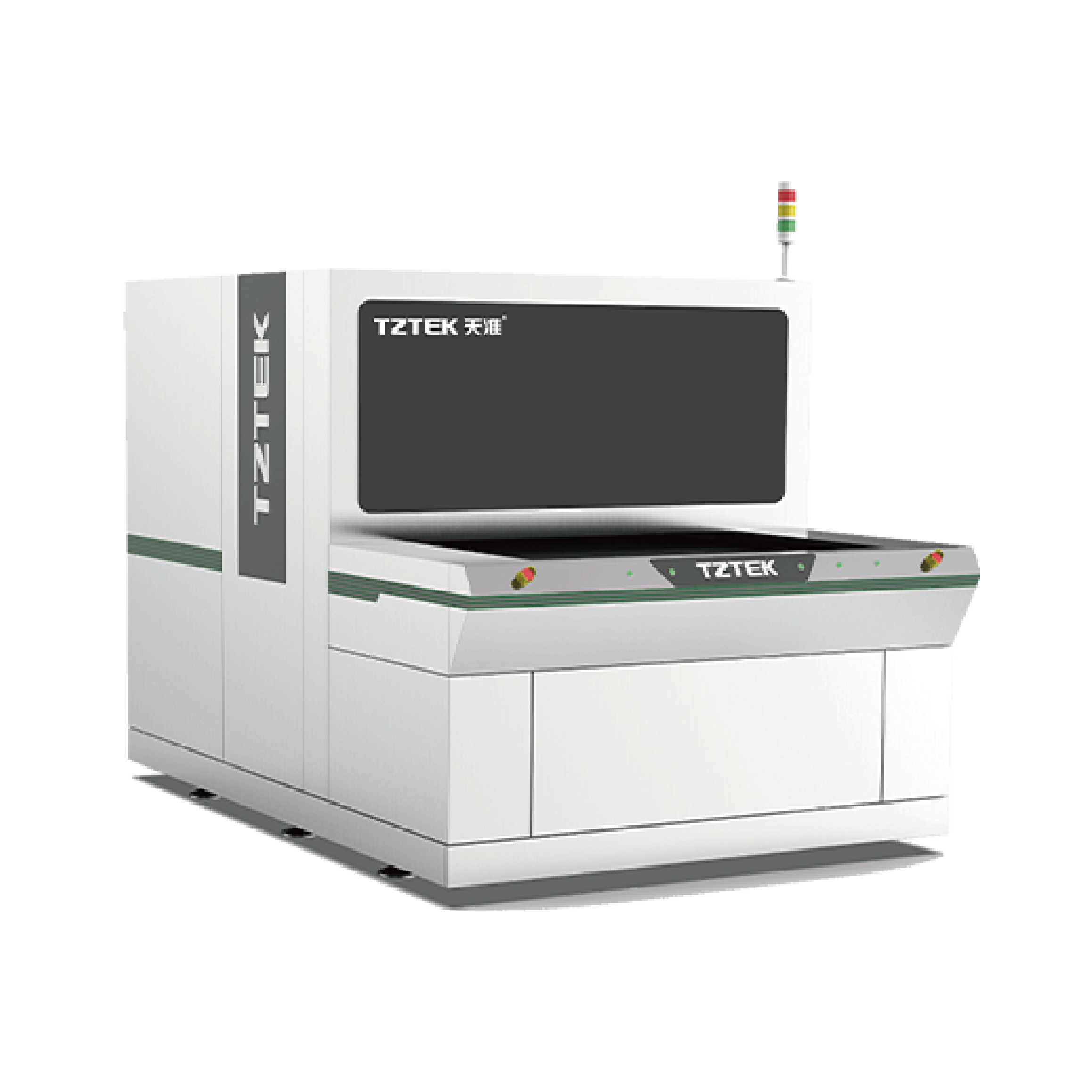
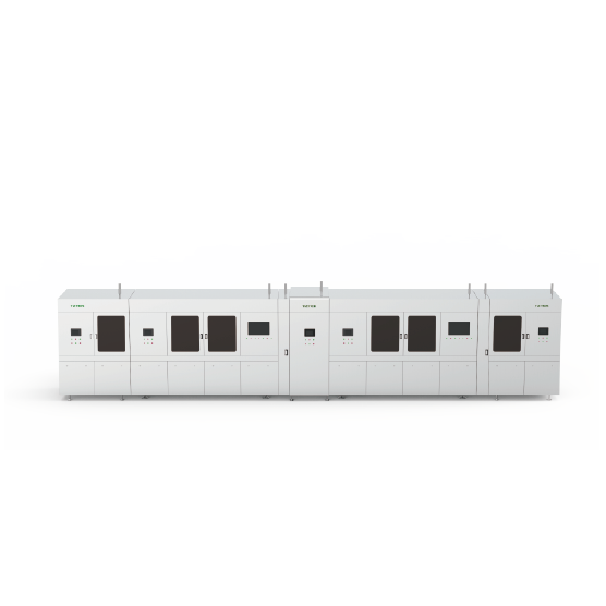
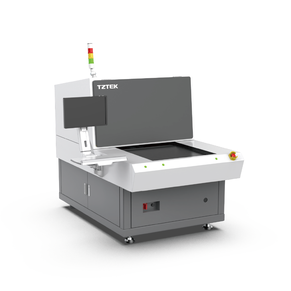
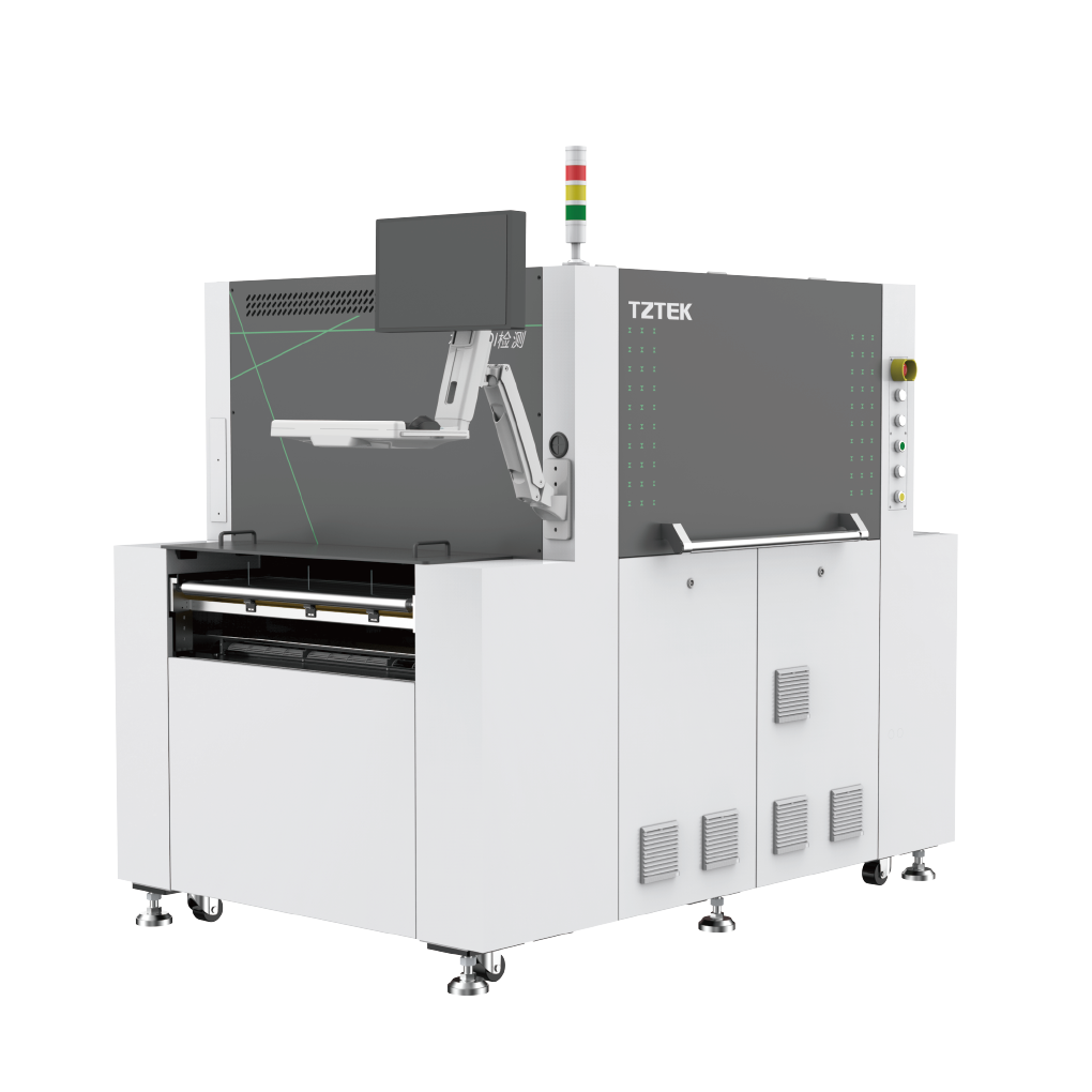
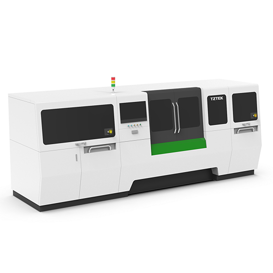
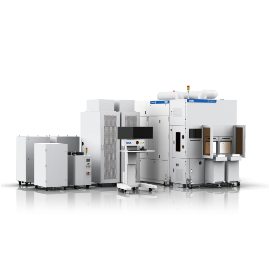
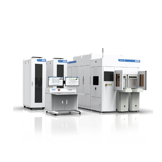
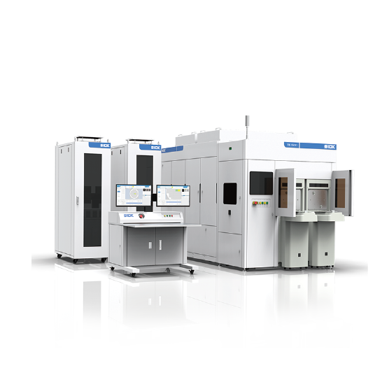
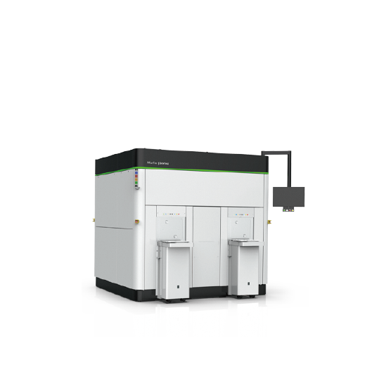
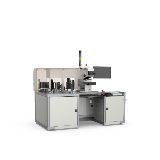
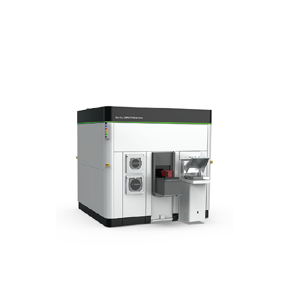
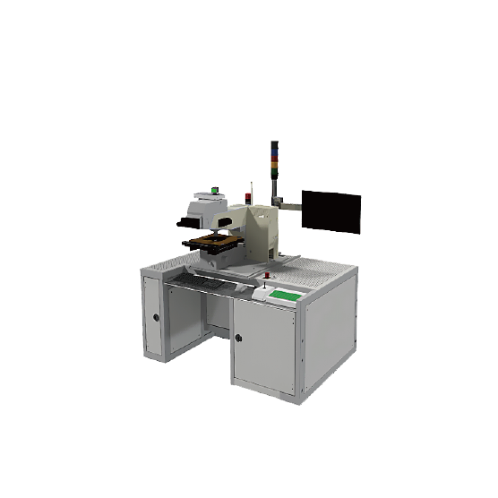
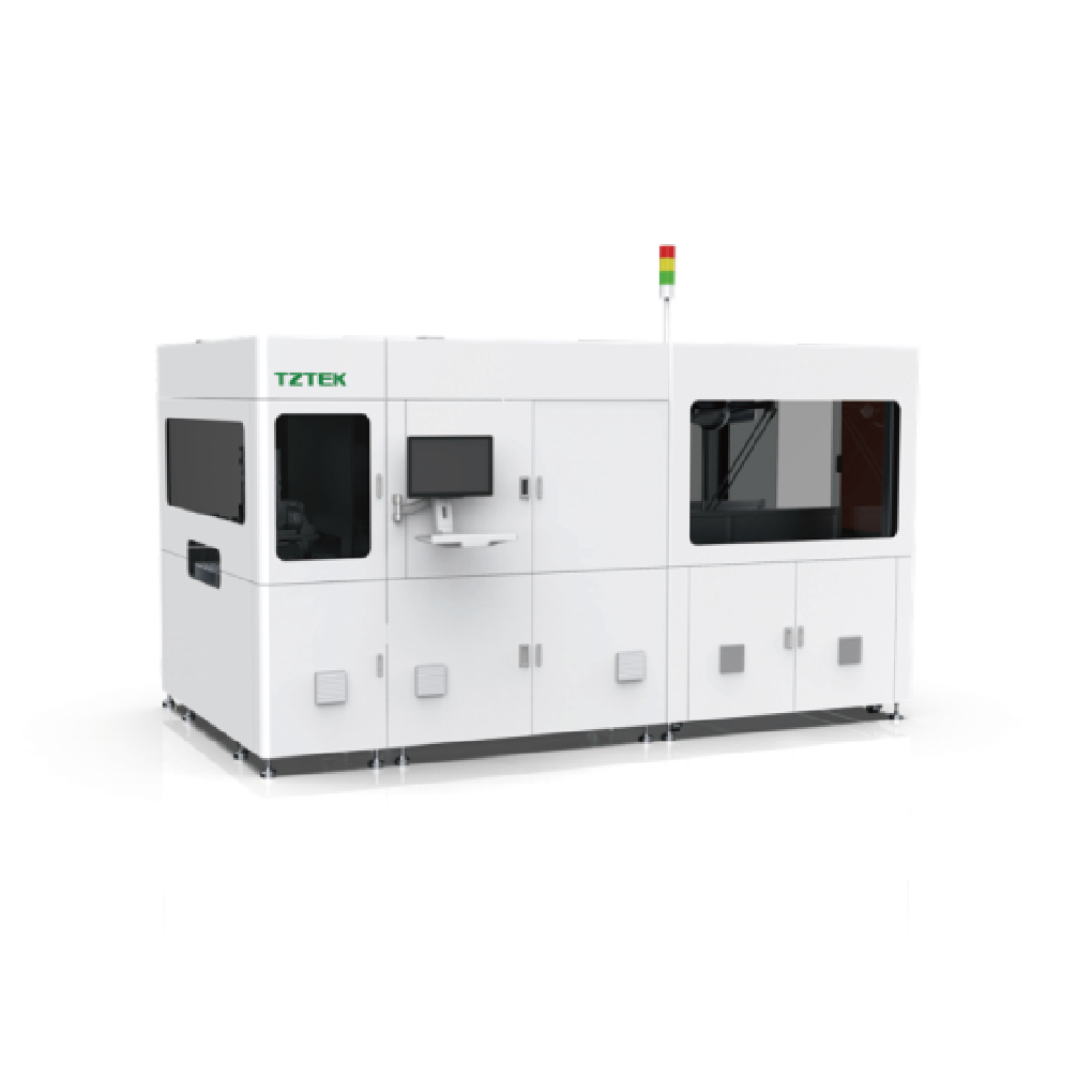
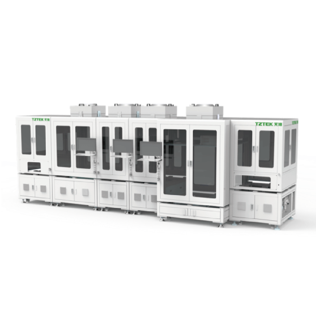
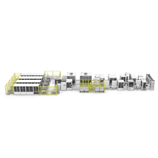
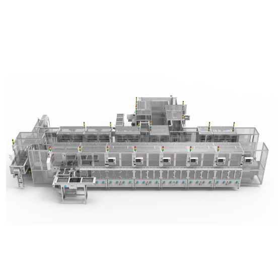
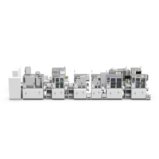
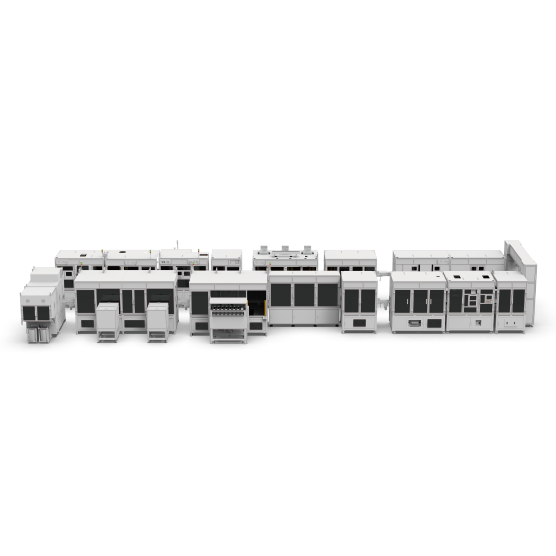
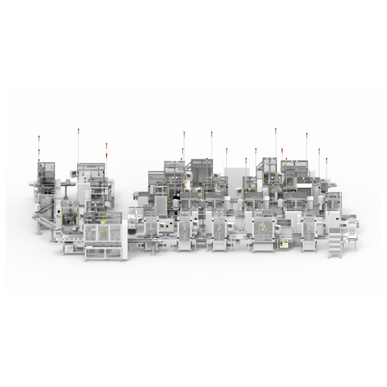
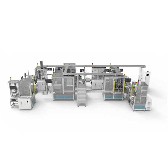
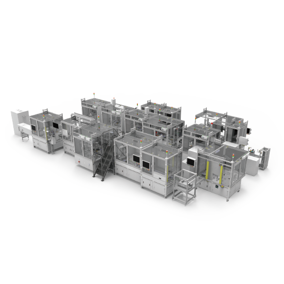
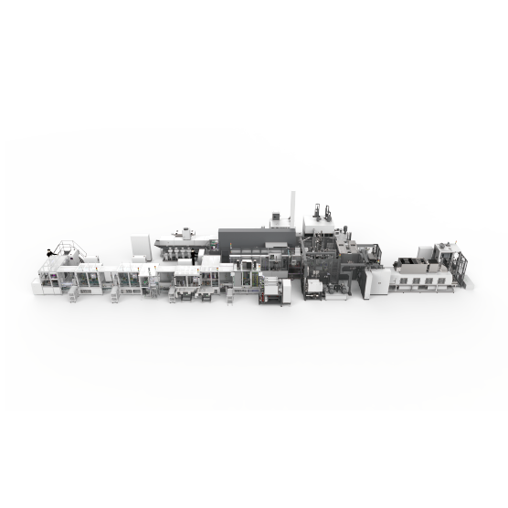
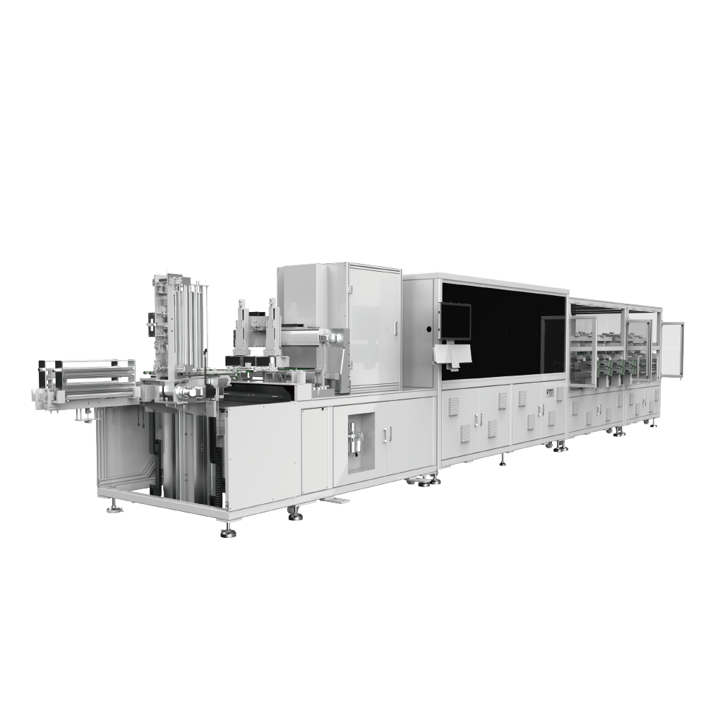


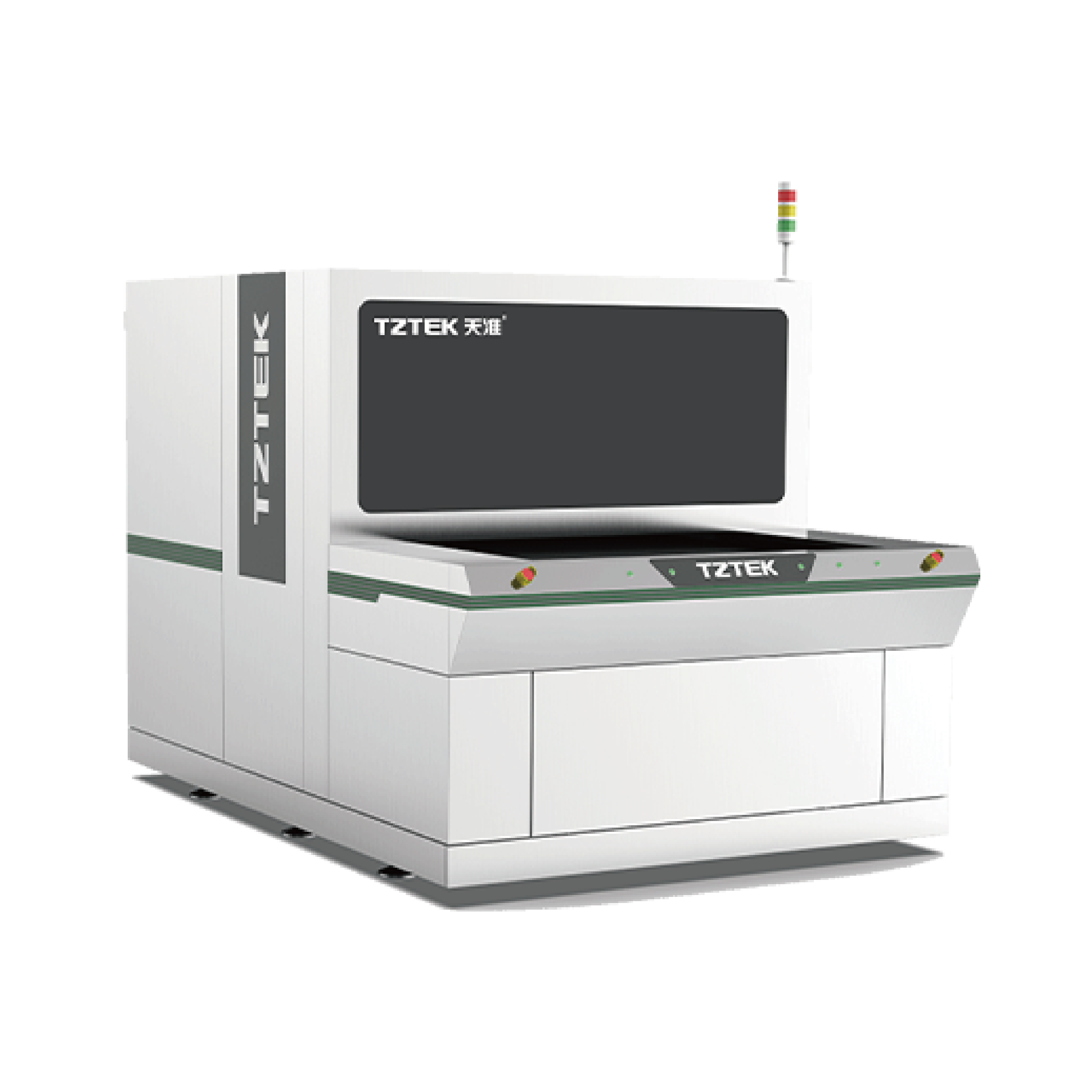
IC Substrate LDI Equipment


Training Certificate Inquiry
Advantages
-
High Precision
-
Powerful Functions
-
High Throughput
-
Intelligent Operation
-
 High Precision
Registration accuracy up to ±5 μm
Minimum line/space down to 4/4 μm

-
 Powerful Functions
Active autofocus for dynamic substrate deformation compensation
Hybrid UV LED and laser light source technology for a wide range of solder mask curing requirements in package substrate manufacturing
Real-time laser energy monitoring with automatic compensation
-
 High Throughput
High-throughput data processing solution
Simultaneous multi-camera registration for improved multi-zone registration efficiency
-
 Intelligent Operation
Customizable MES integration for real-time equipment management
PC and mobile-based alarms and notifications
PRODUCT SPECIFICATIONS
-
TZDI-06

-
TZDI-04
-

-
Platform Type
Dual-table
-
Maximum Exposure Area
630 mm x 810 mm
-
Substrate Thickness
0.025-6 mm
-
Minimum Line/Space
6 μm
-
Line Width Tolerance
±1 μm
-
Registration Accuracy
±6 μm
-
Interlayer Registration Accuracy
12 μm
-
Depth of Foucs
±75 μm
-
Standalone Throughput
30 s/side @ 20 mJ/cm²
-
Inline Throughput
30 s/panel @ 20 mJ/cm²
-
Recommended Applications
IC substrate
-
-
-
Platform Type
Single-table
-
Maximum Exposure Area
630 mm × 610 mm
-
Substrate Thickness
0.025-5 mm
-
Minimum Line Width
4/4 μm
-
Line Width Tolerance
±0.75 μm
-
Registration Accuracy
±5 μm
-
Interlayer Registration Accuracy
10 μm
-
Depth of Focus
±200 μm (Optional Active Focusing)
-
Standalone Throughput
60 s/side @100 mJ/cm²
-
Recommended Applications
ICS, SLP
-