




Overlay & Critical Dimension (CD) Metrology
INDUSTRY CHALLENGES
-
 01
01Shrinking Critical Dimensions: Advanced nodes demand tighter CD and overlay control at the nanometer scale.
-
02
Complex Multi-Layer Processes: Multi-layer stacks and hundreds of process steps increase overlay monitoring requirements.
-
03
Complex Device Structures: 3D NAND, FinFET, and GAA introduce new metrology targets beyond conventional measurement approaches.


INDUSTRY SOLUTION
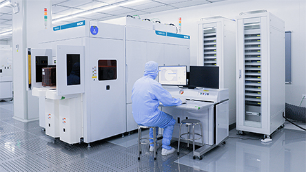
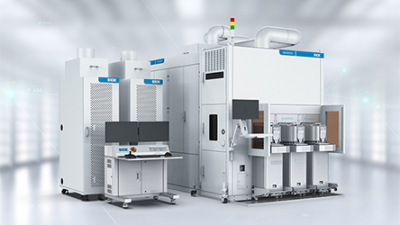
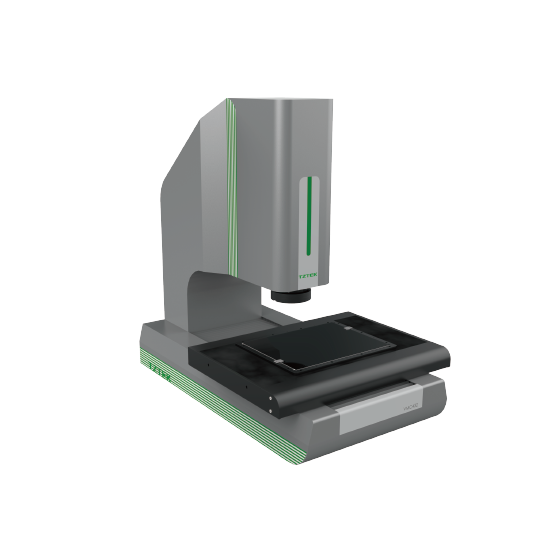
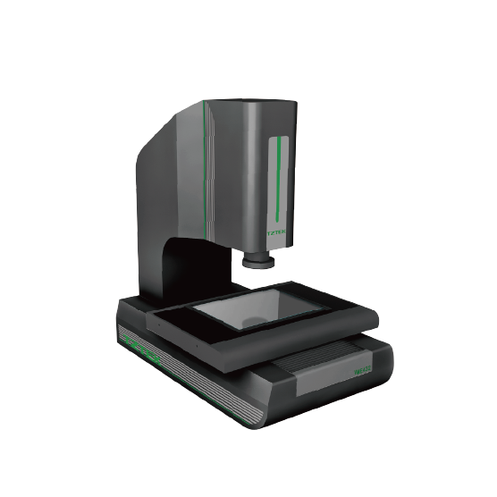
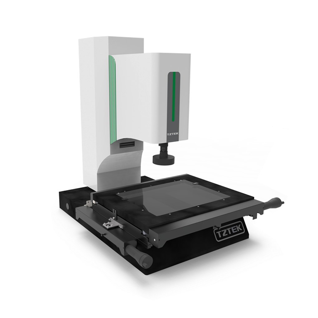
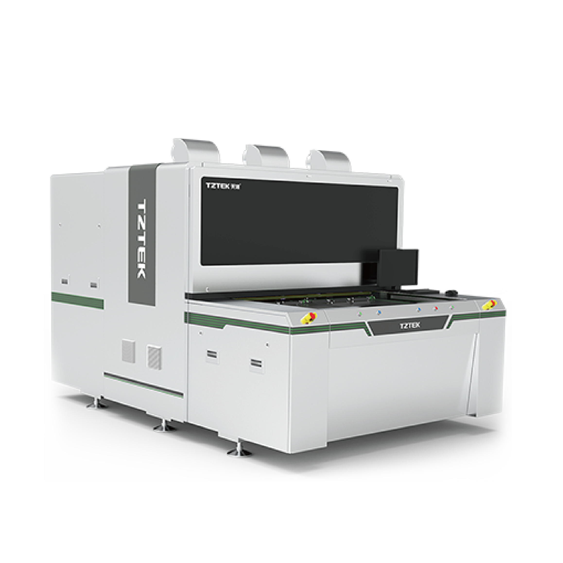
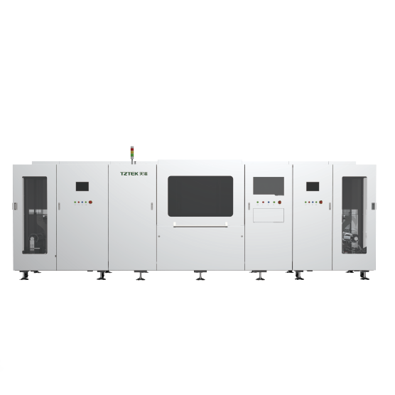
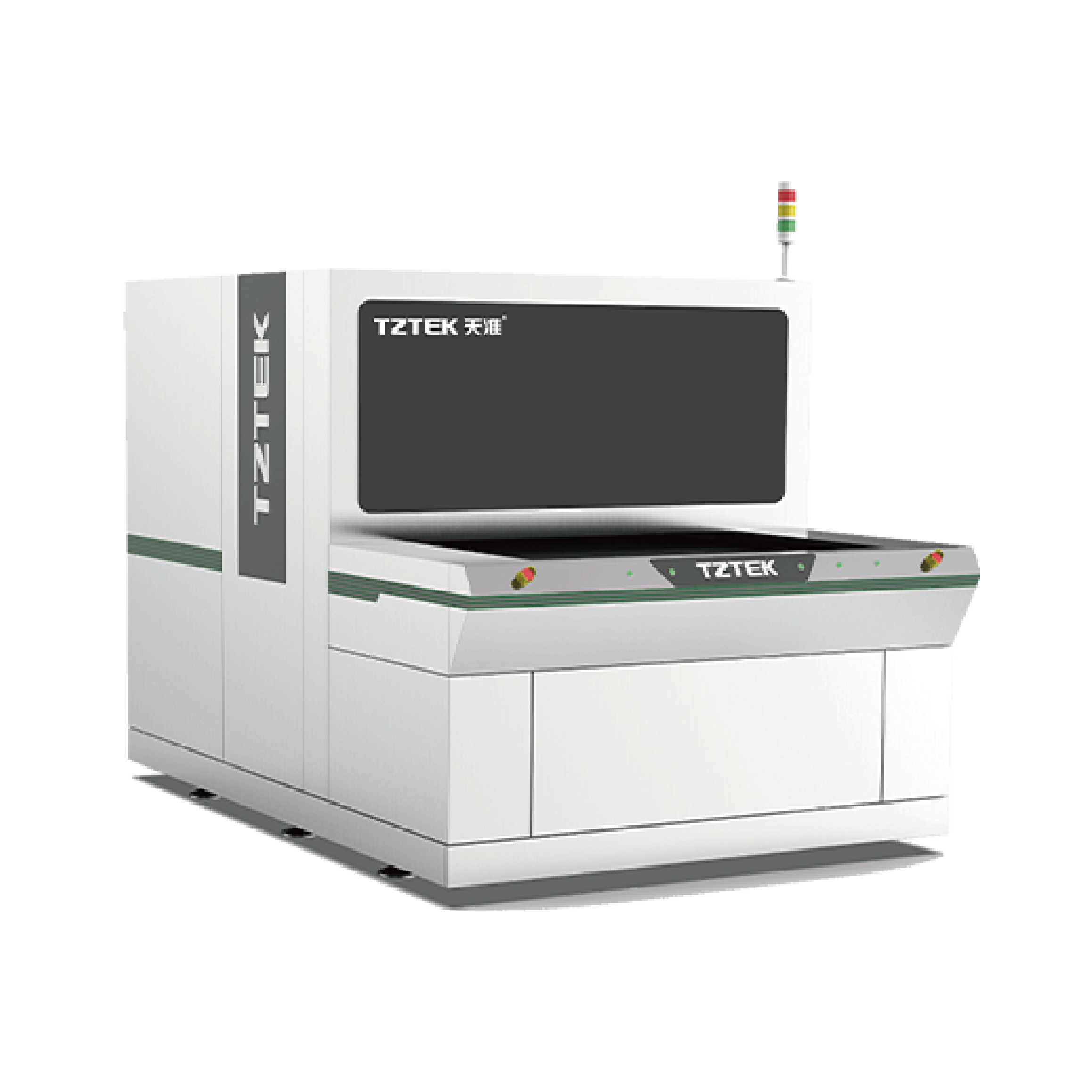
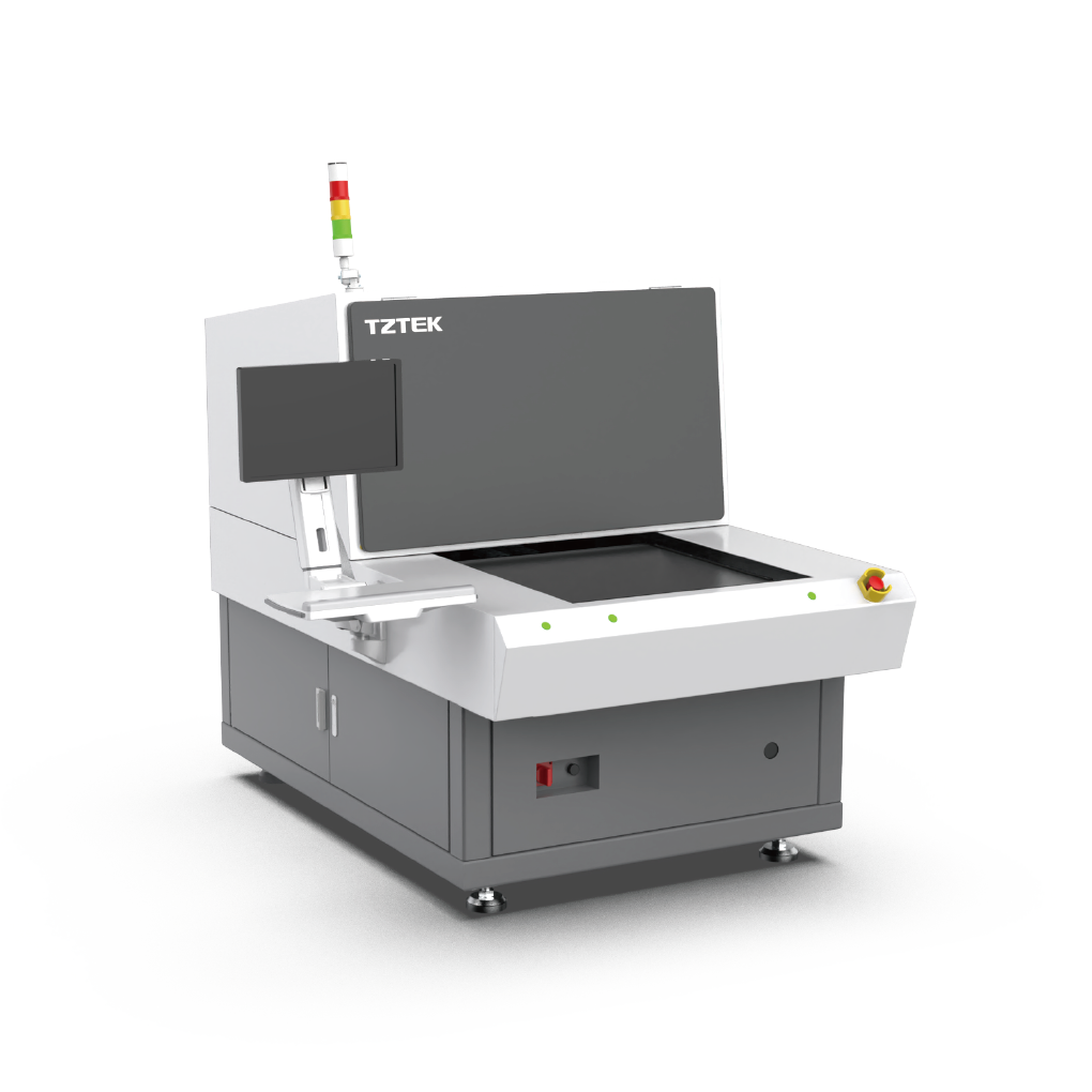
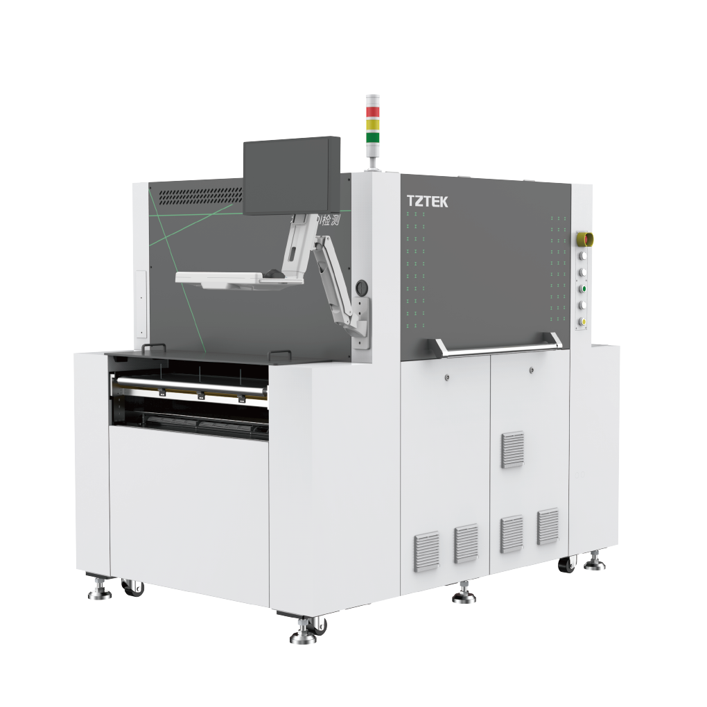
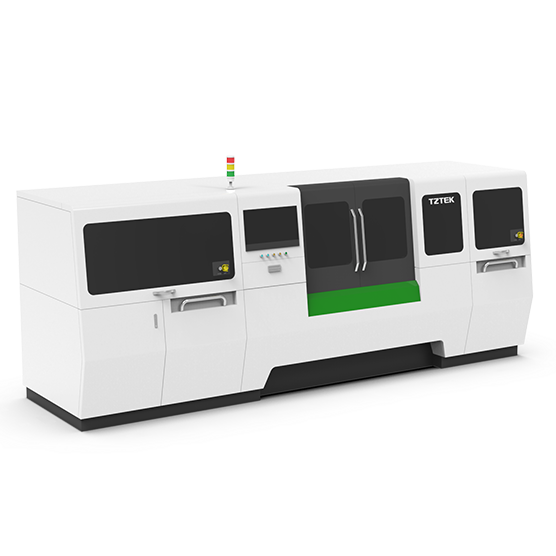
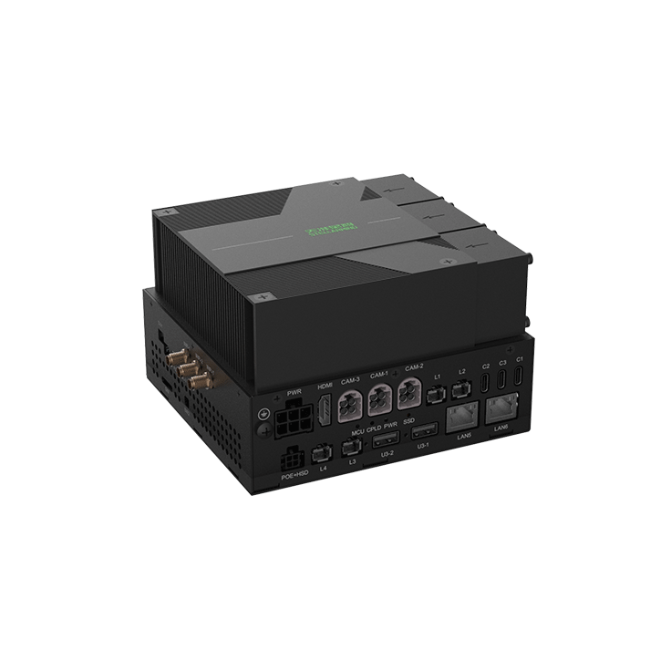
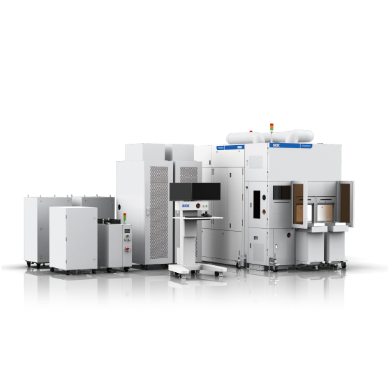
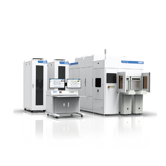
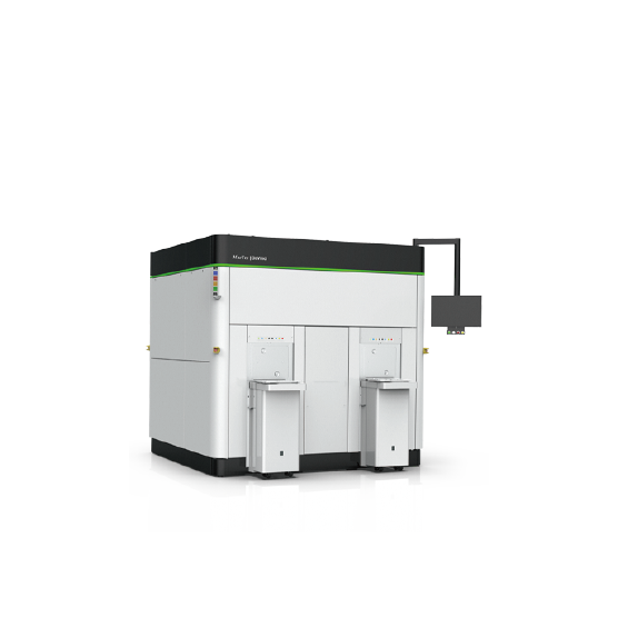
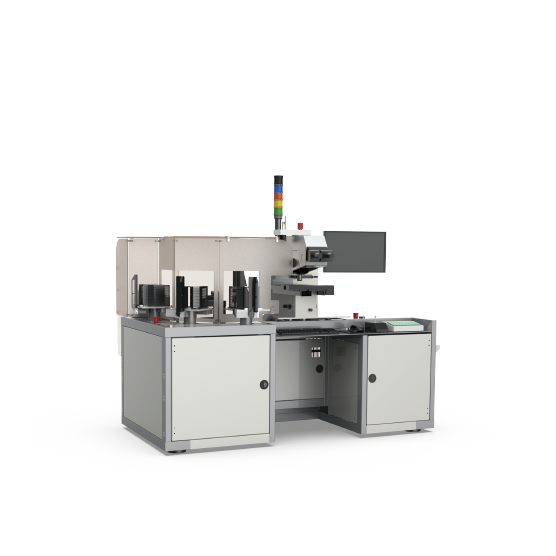
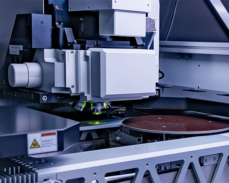
TZTEK combines the DaVinci Overlay Metrology System and MT3000VIS/UV Wafer Metrology Platform for comprehensive, high-precision metrology across front-end processes.
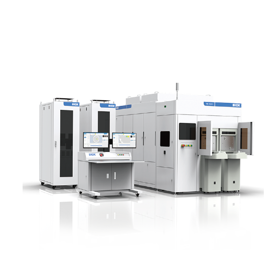
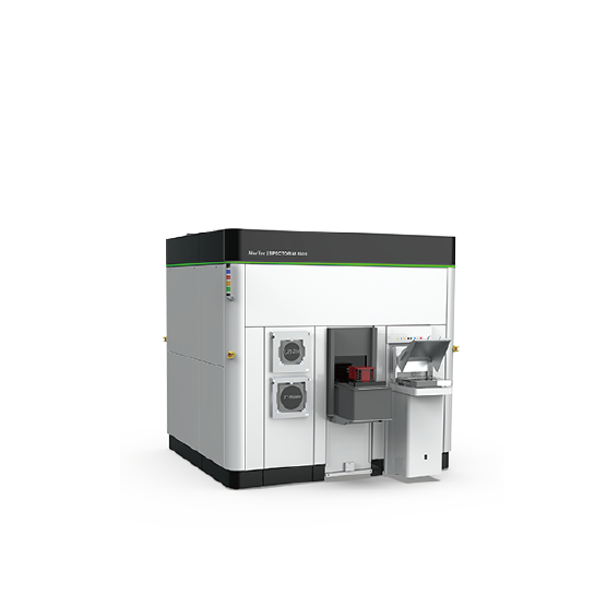
DaVinci Overlay Metrology System: Fully automated sub-nanometer overlay metrology for 200 mm and 300 mm wafers, with automatic recipe generation and SECS/GEM connectivity for high-volume manufacturing.
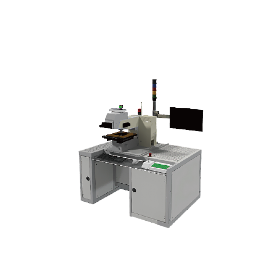
MT3000 Wafer Metrology Platform: Automated CD, overlay, and thin-film thickness measurement for wafers up to 200 mm—from front-end wafer processing to advanced packaging. Overlay repeatability: 1.5 nm, typically 1.0 nm. CD repeatability: 3 nm, typically 2 nm. Automated handling supports R&D and high-volume process monitoring.
KEY ADVANTAGES
-


Sub-Nanometer Accuracy: DaVinci delivers overall measurement accuracy down to the sub-nanometer level.
-

Integrated Metrology: CD, overlay, and thin-film thickness measurement on a single platform, supporting multiple wafer sizes.
-

Reliability & Low COO: Easy maintenance, no short-cycle consumables, and over a decade of customer validation.