




Circuit & Solder Mask Imaging
INDUSTRY CHALLENGES
-
 01
01MSAP and advanced IC substrate applications are pushing line/space below 25 μm, demanding higher imaging resolution and registration accuracy.
-
02
More complex stack-ups and substrate dimensional variation make consistent layer-to-layer registration increasingly difficult.
-
03
High-volume production and smart manufacturing demand high-speed imaging, equipment connectivity, data monitoring, and production analytics.


INDUSTRY SOLUTION
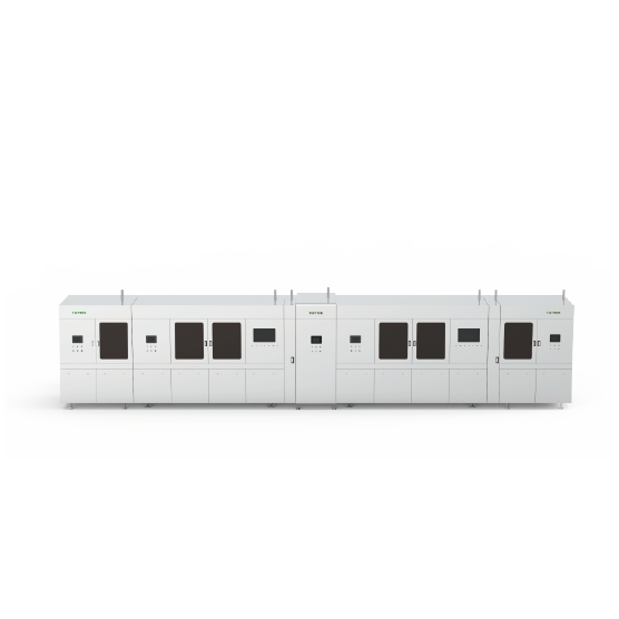
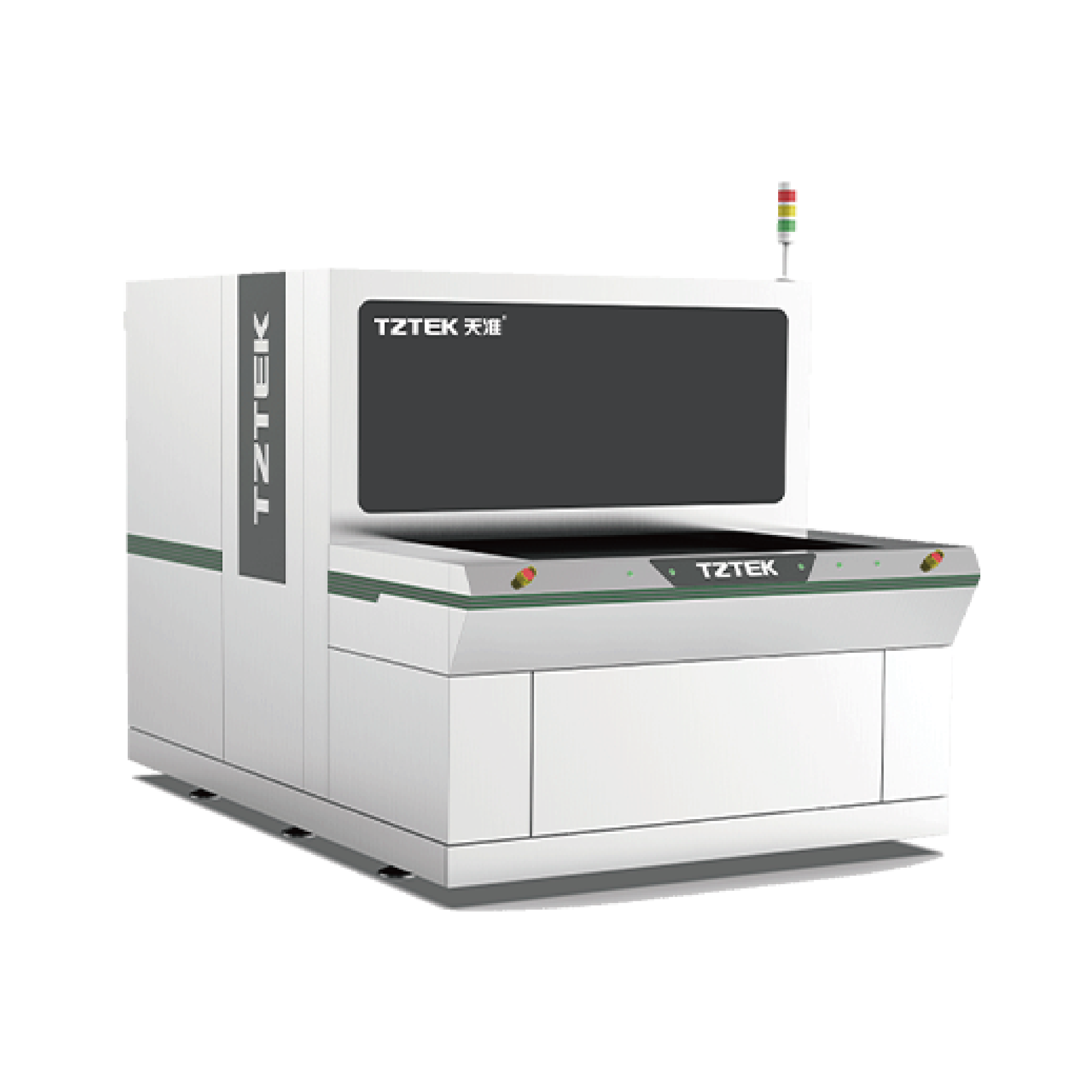
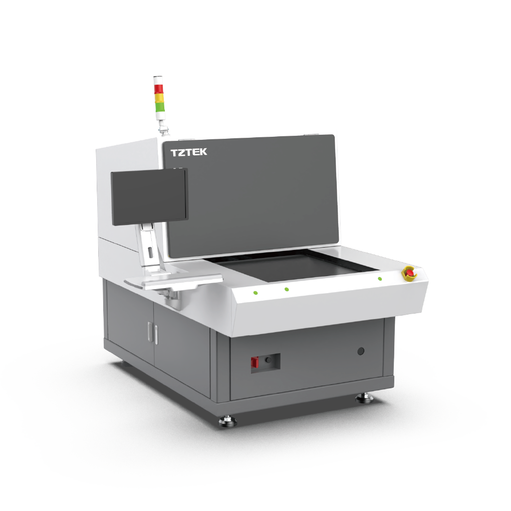
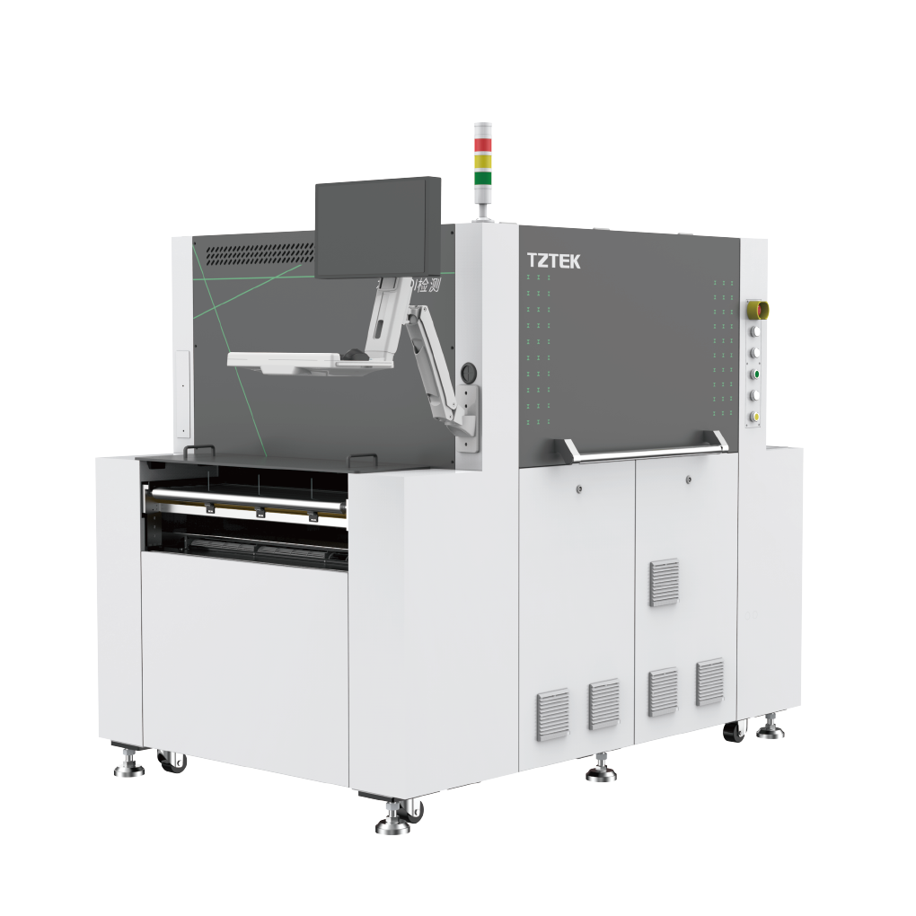
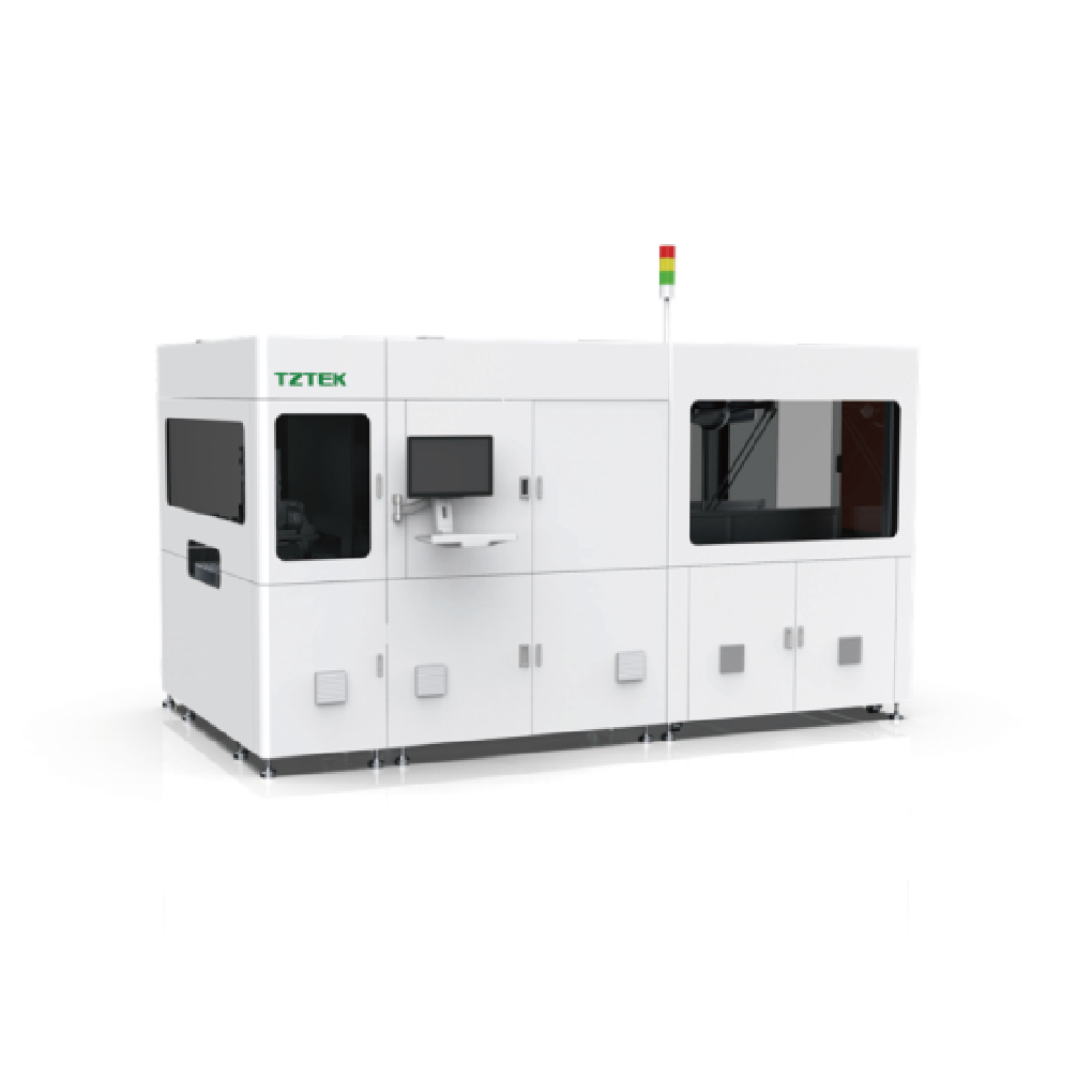
LDI is critical to fine-line patterning and layer-to-layer registration in high-density PCB manufacturing, directly impacting pattern quality and production yield.
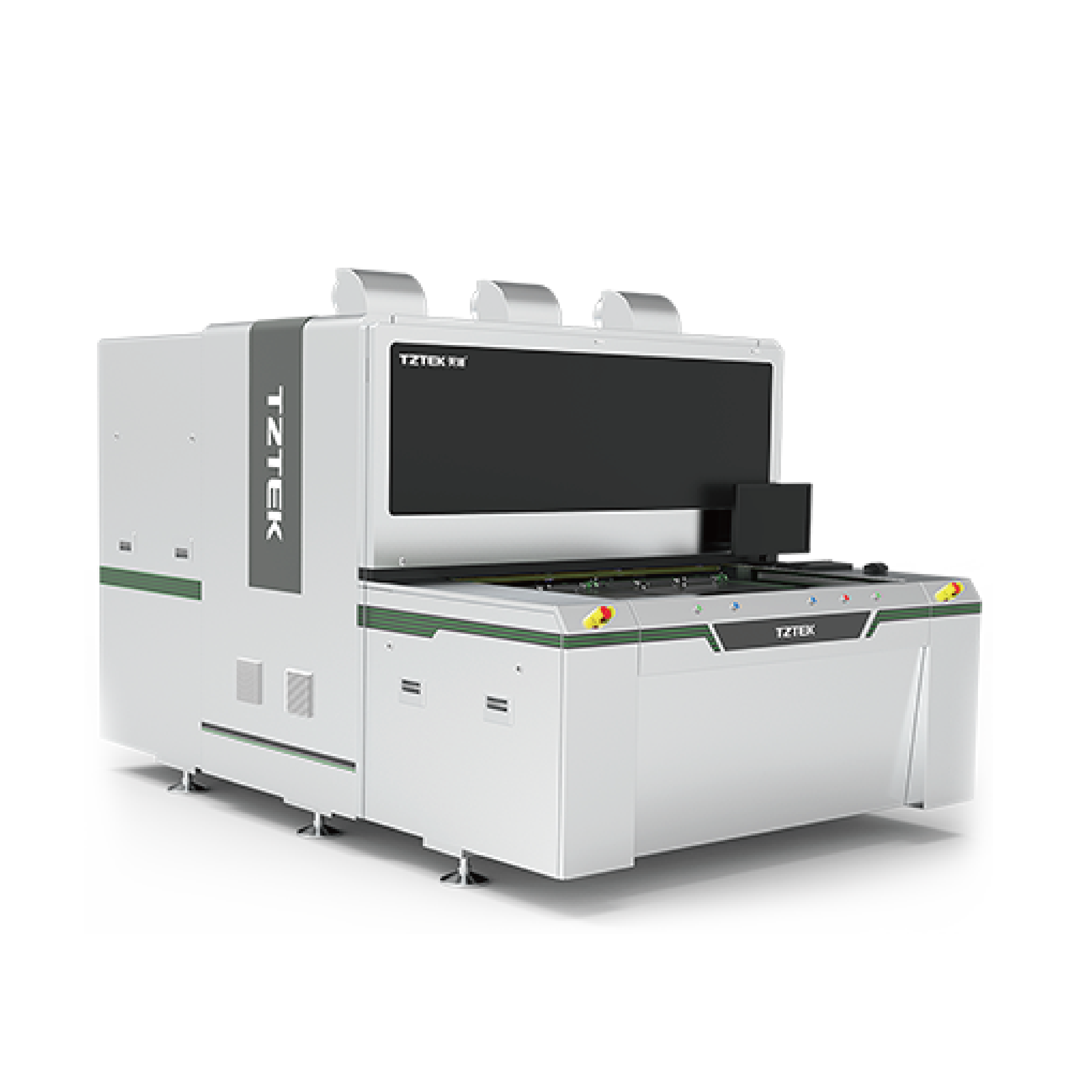
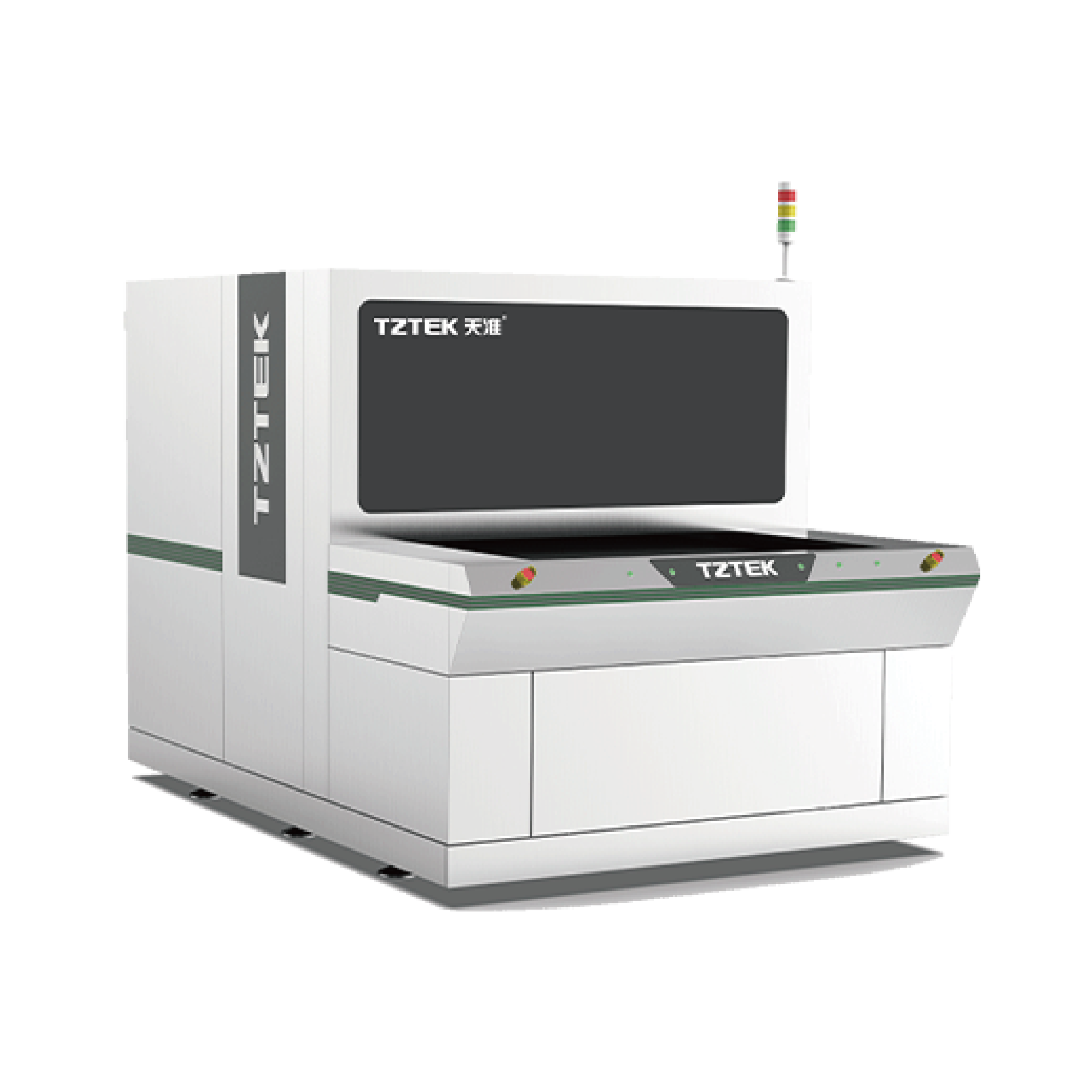
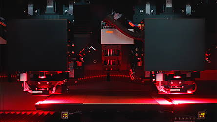
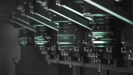
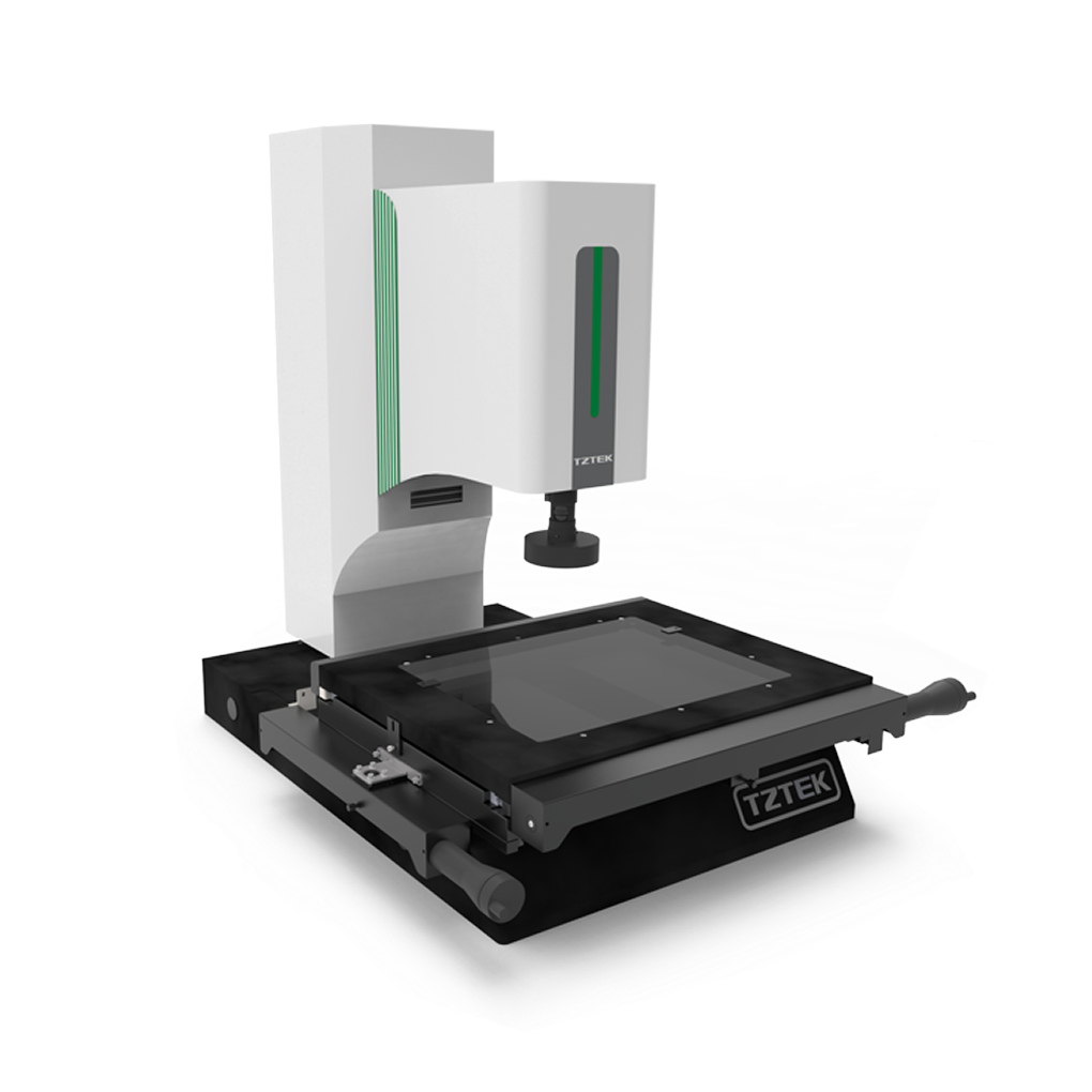
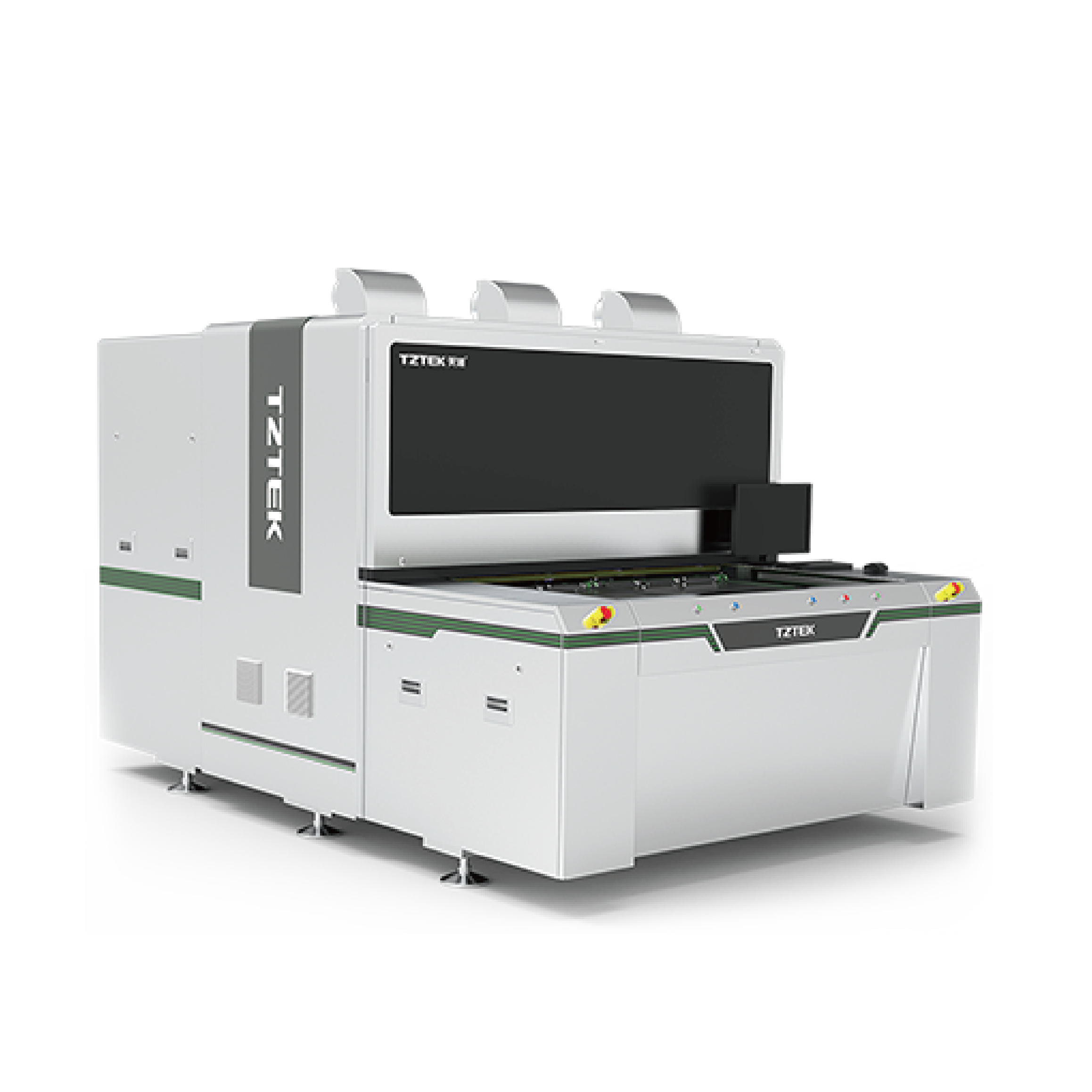
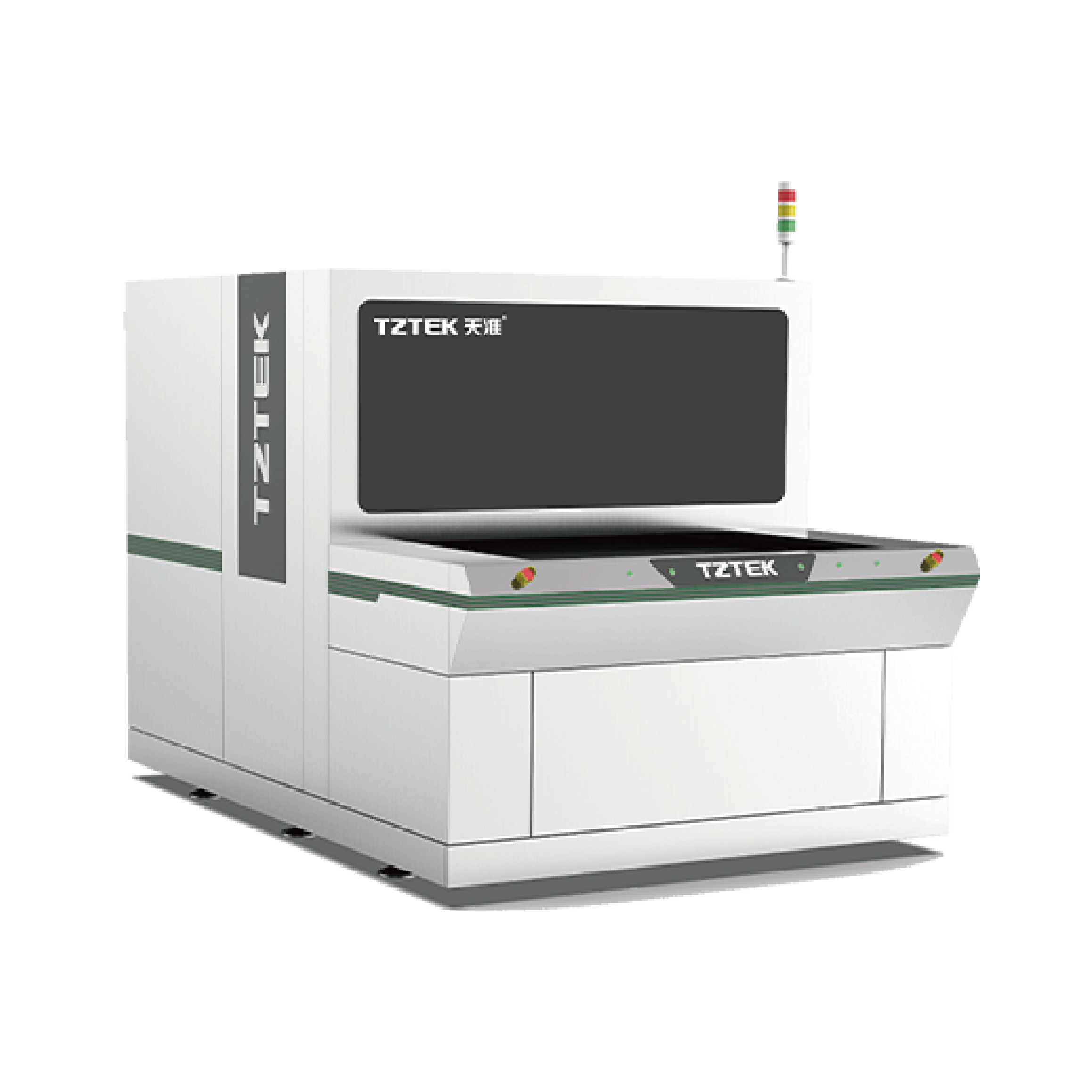
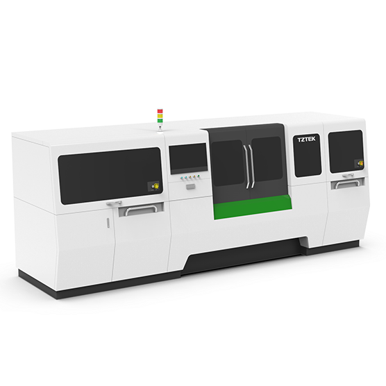
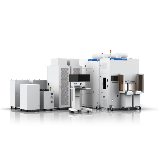
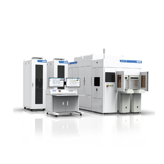
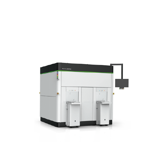
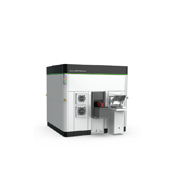
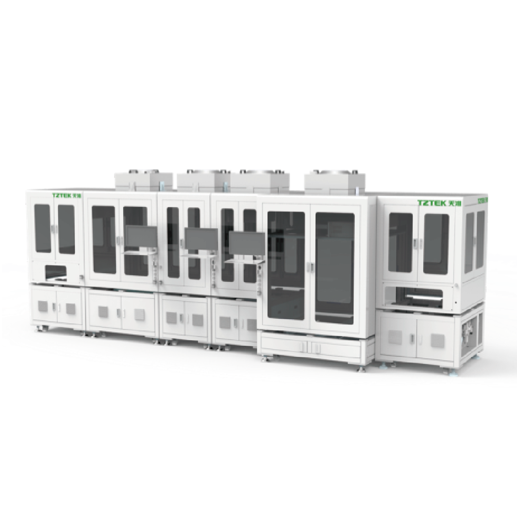
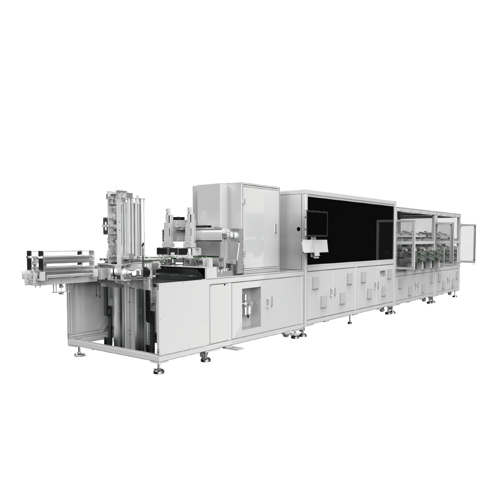
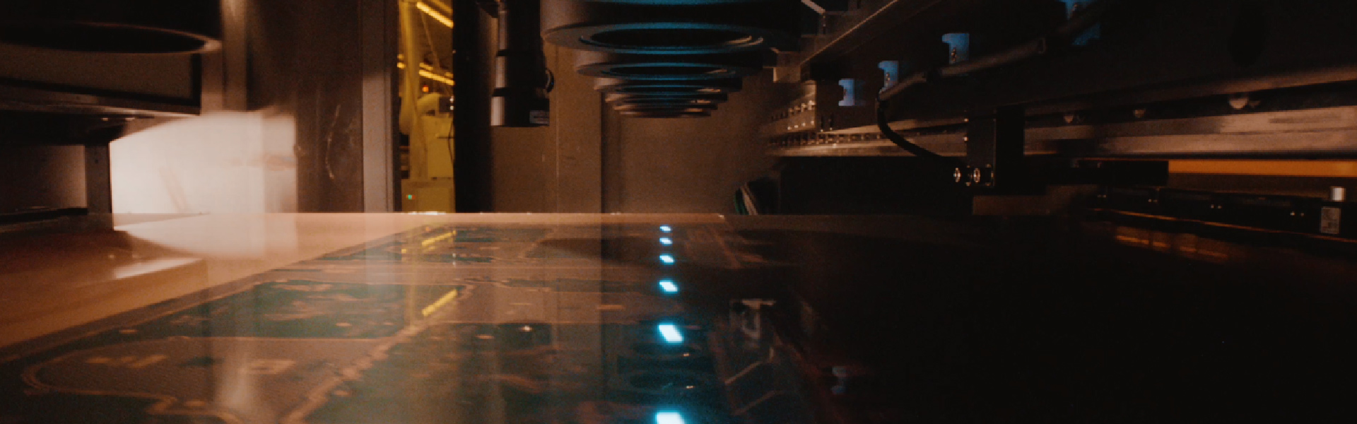
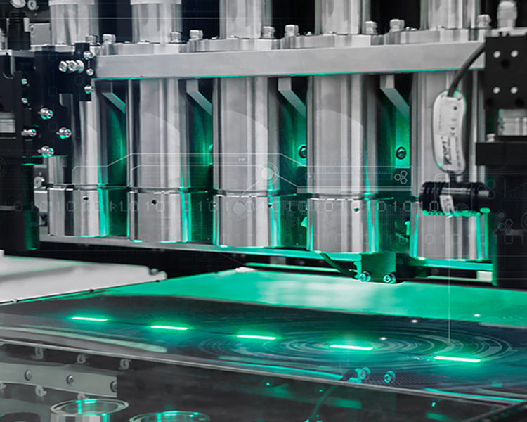
TZTEK's LDI combines proprietary high-resolution optics and parallel multi-beam scanning to deliver 4 μm line/space imaging with ±5 μm registration accuracy.
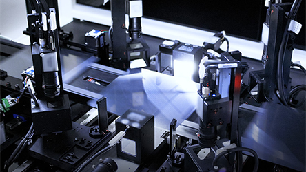
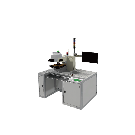
High-precision CCD multi-point alignment and intelligent distortion compensation dynamically correct substrate dimensional variation for consistent layer-to-layer registration.
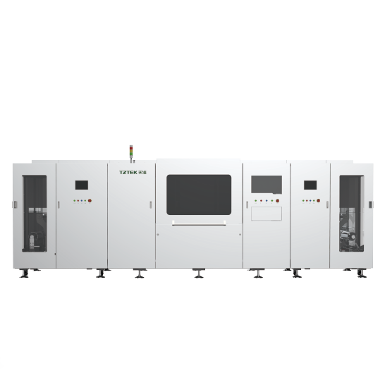
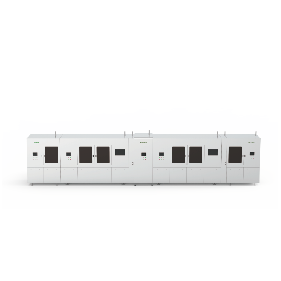
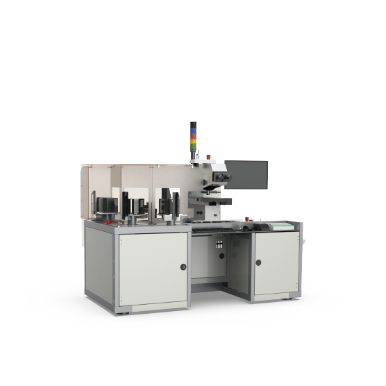
High-speed scanning supports high-volume production, while an integrated manufacturing management platform enables CAM data import, real-time process monitoring, and full data traceability.
KEY ADVANTAGES
-


High-resolution imaging and registration accuracy for HDI, IC substrates, and flexible PCBs.
-

High throughput with precision imaging, supporting fast product changeovers for high-volume production.
-

Connected equipment and remote diagnostics, with MES integration and preventive maintenance to minimize downtime.