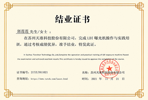



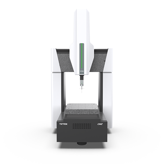
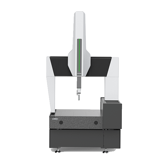
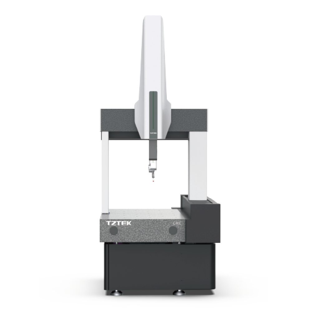
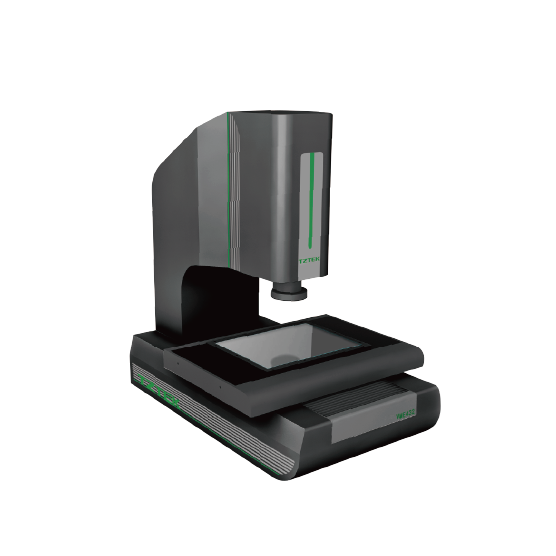
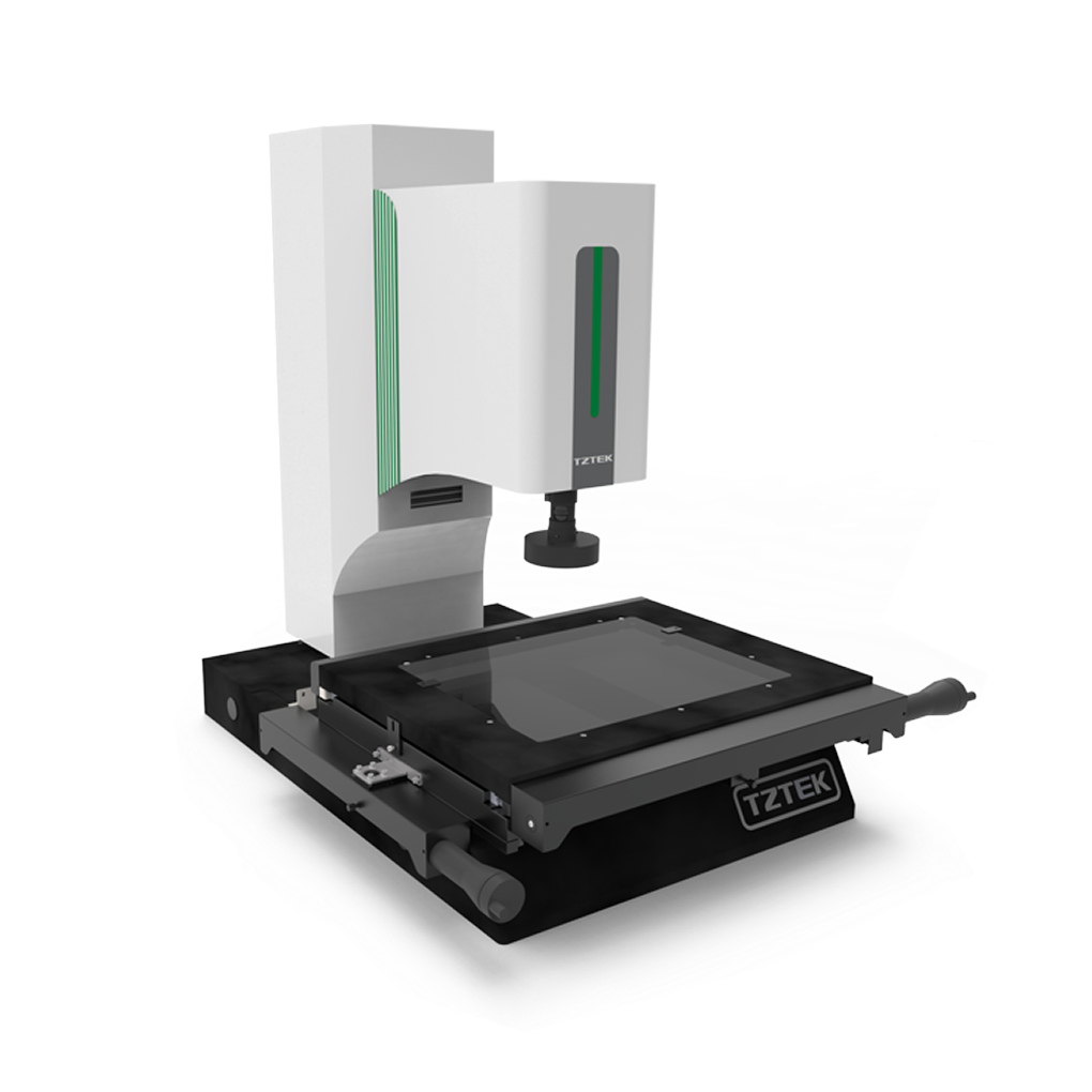
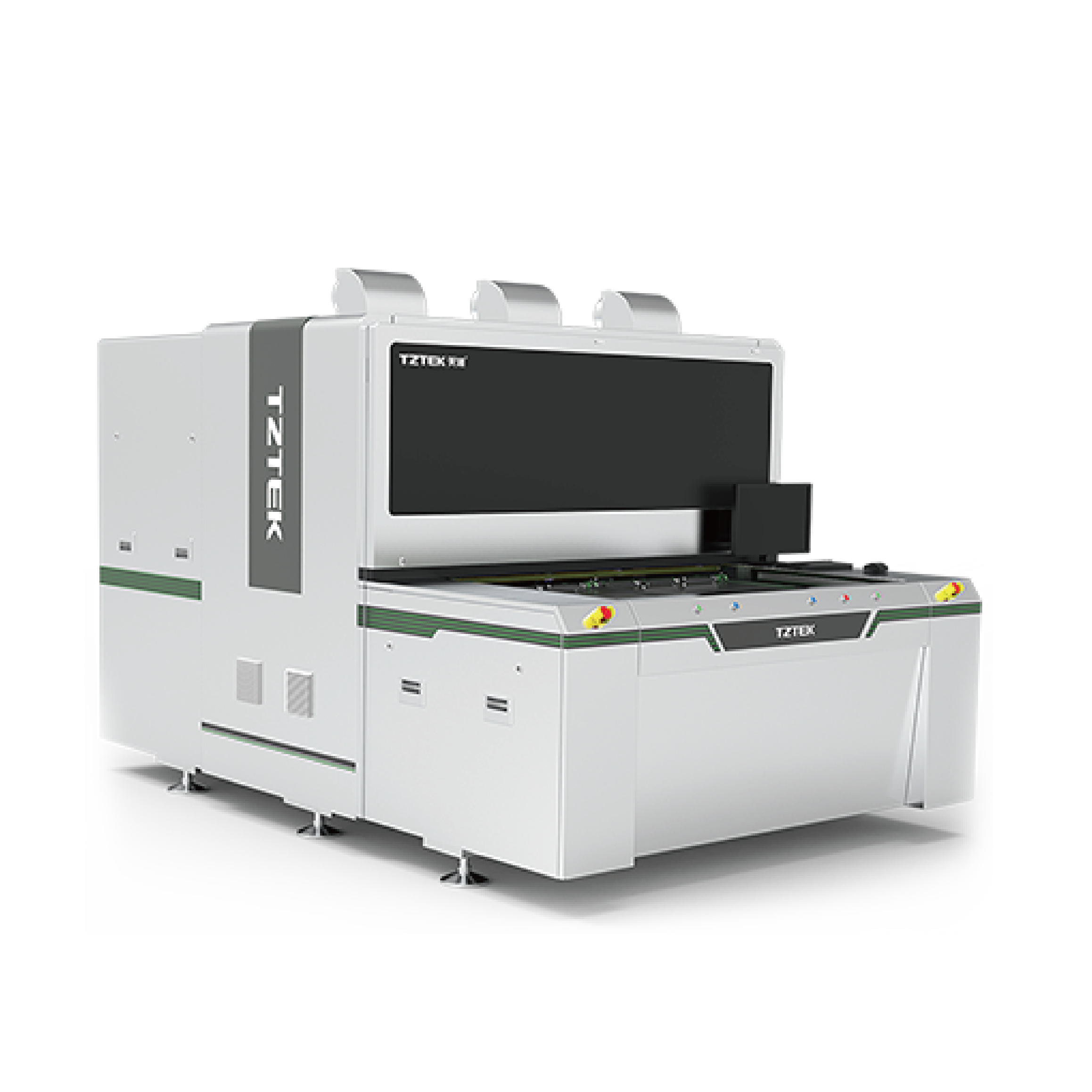
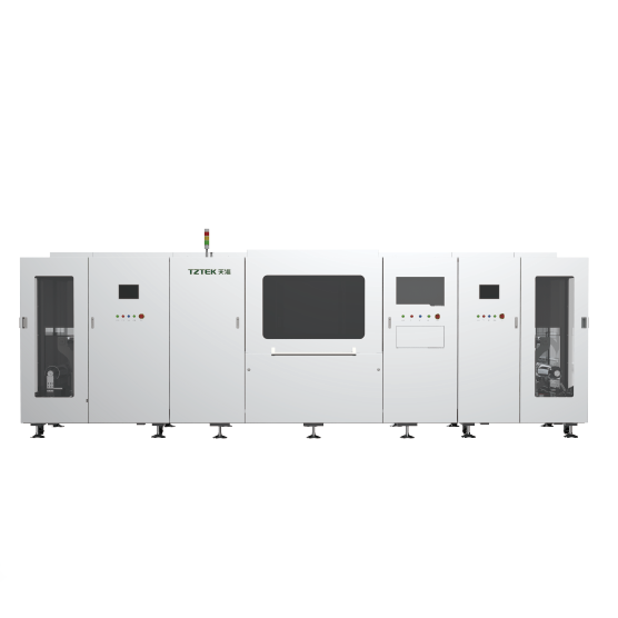
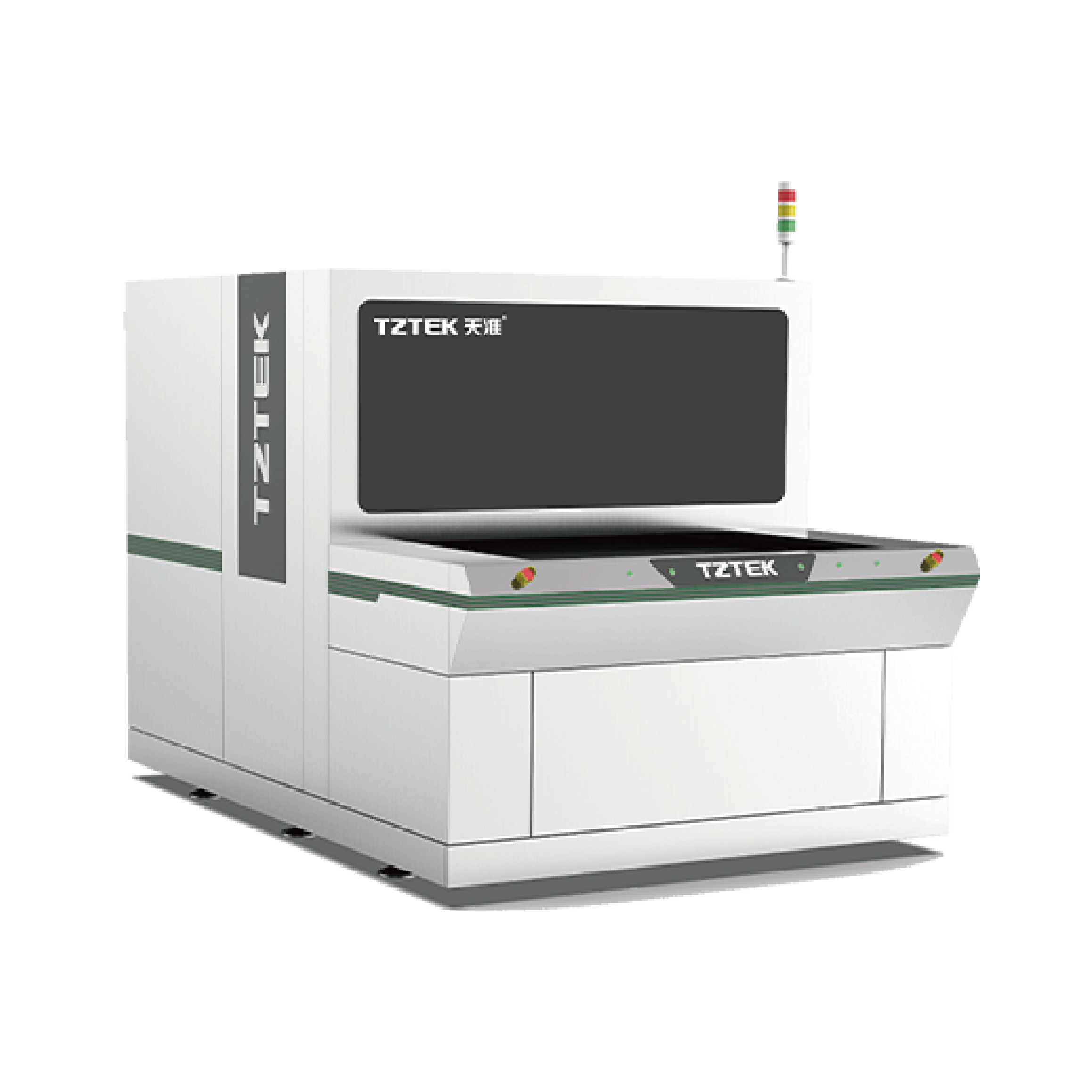
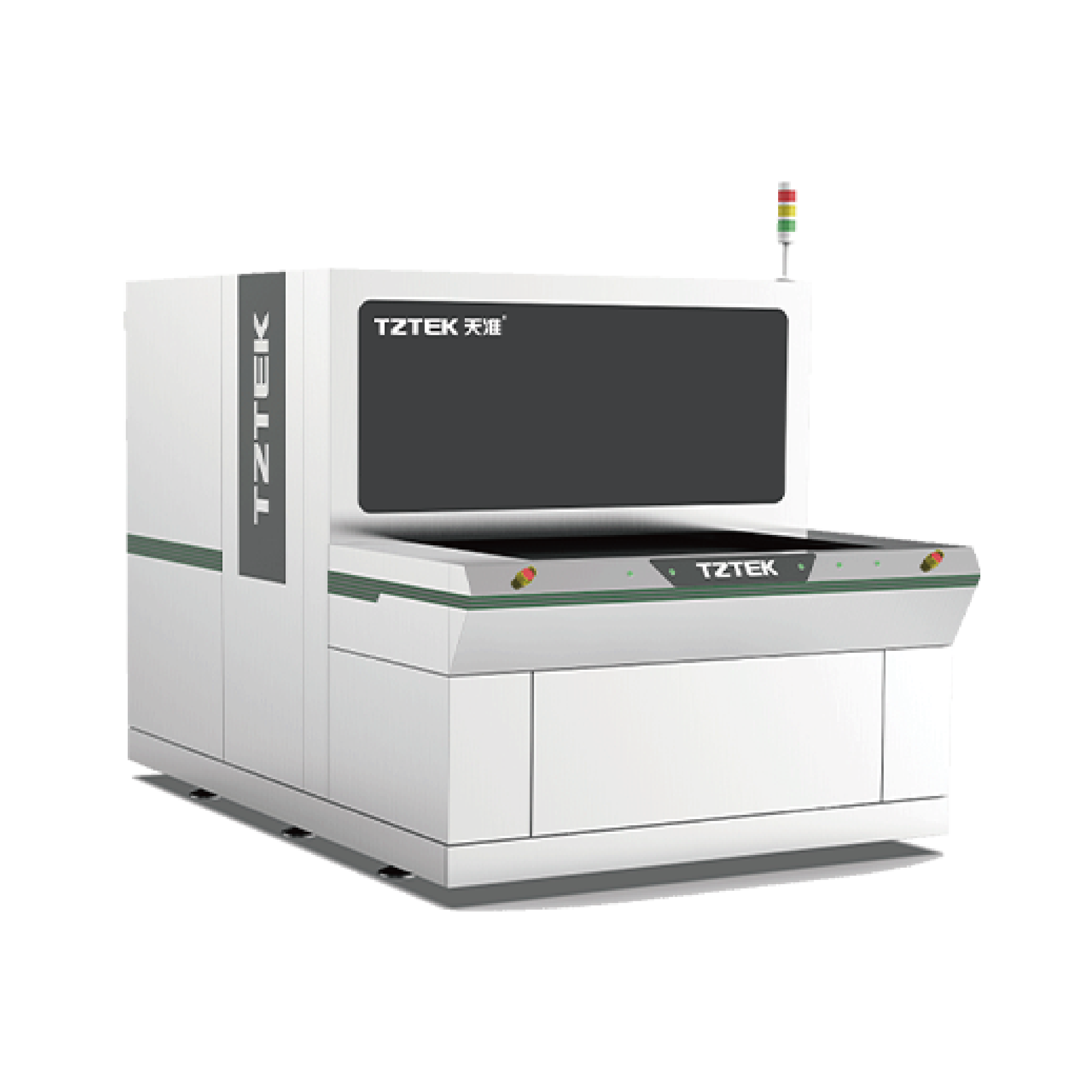
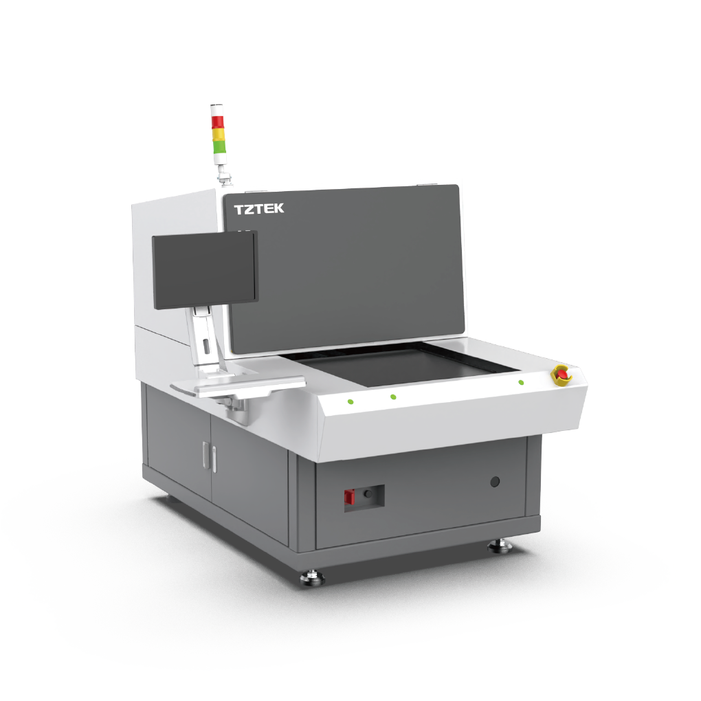
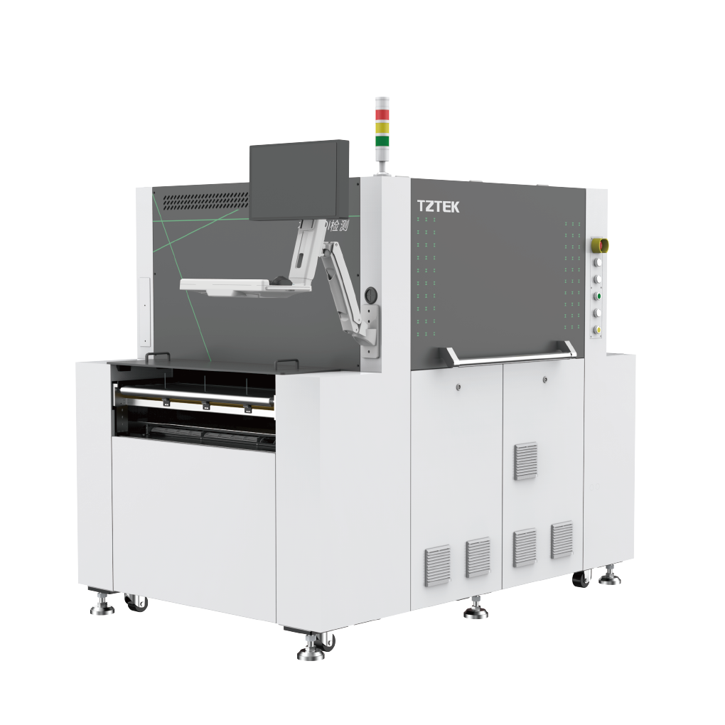
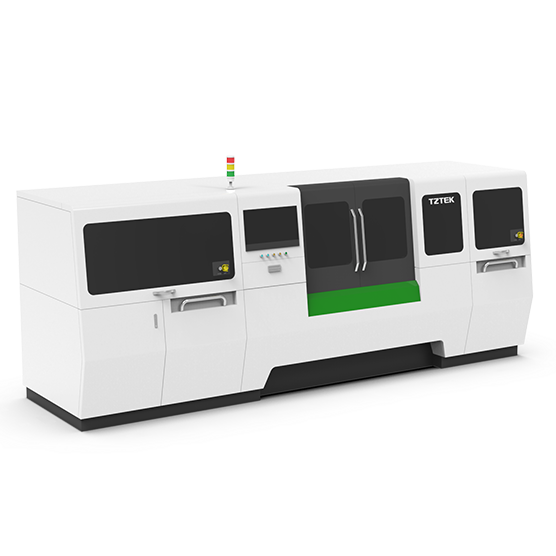
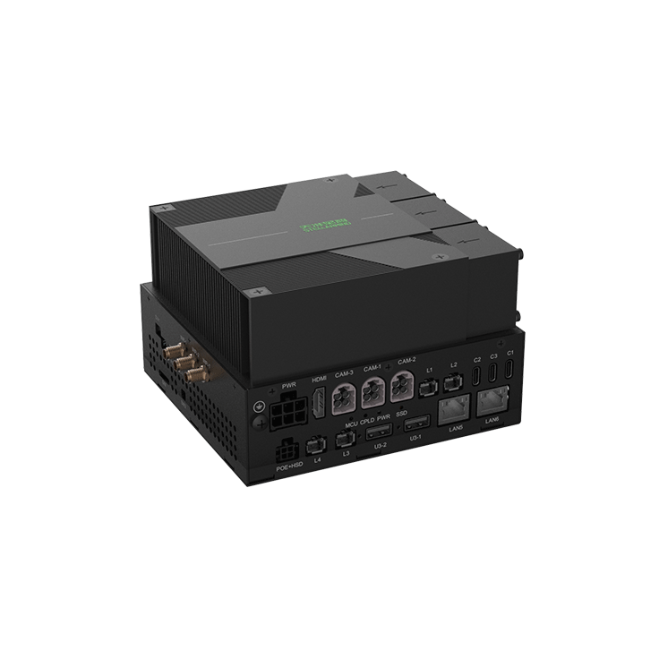
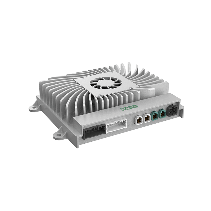
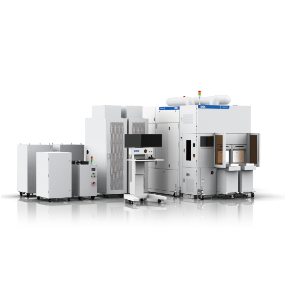
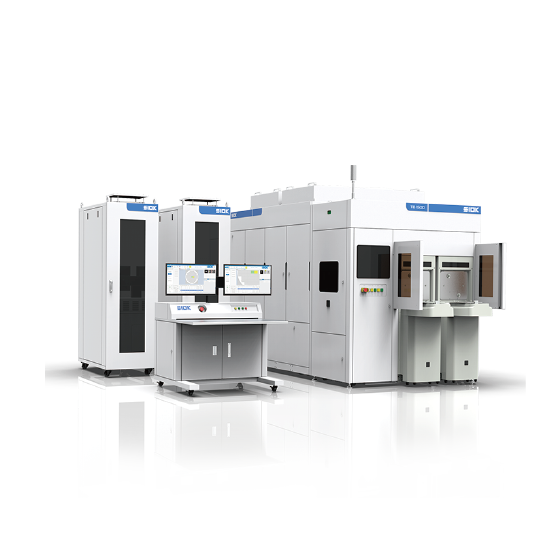
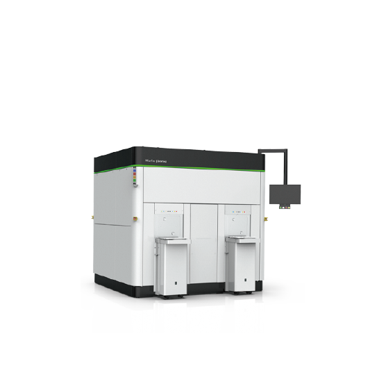
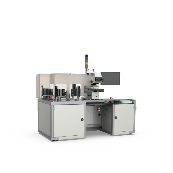
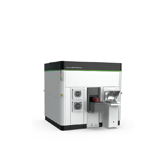
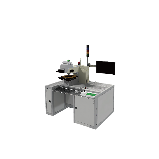
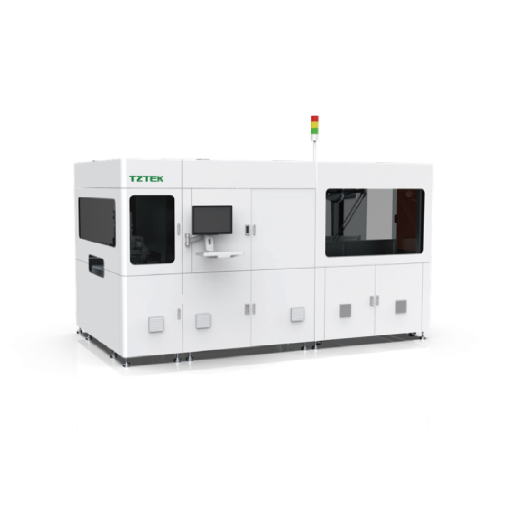
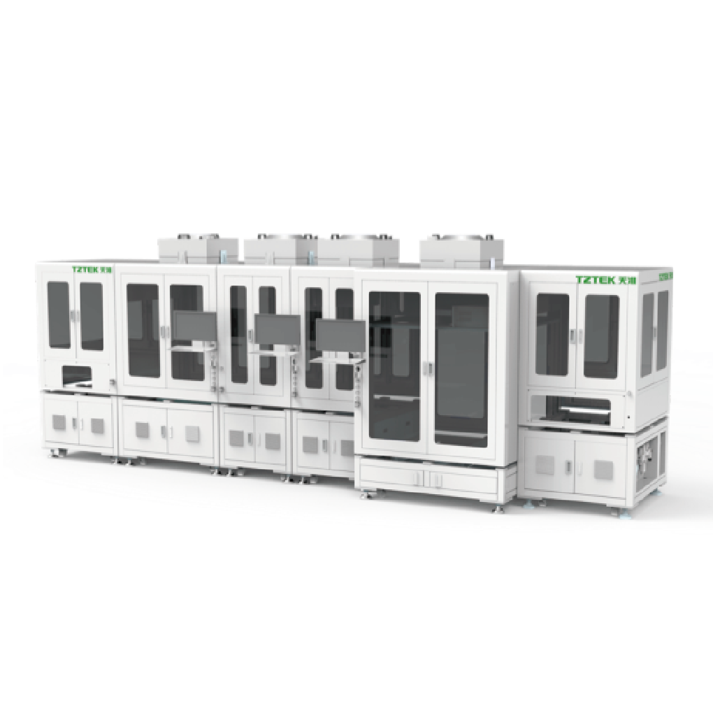
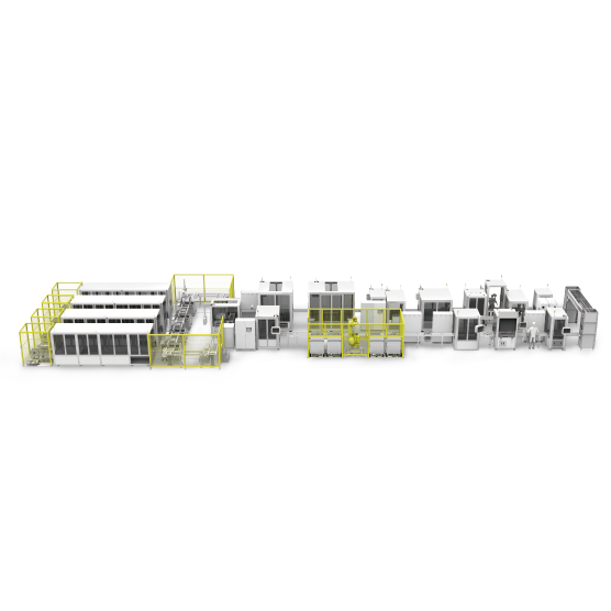
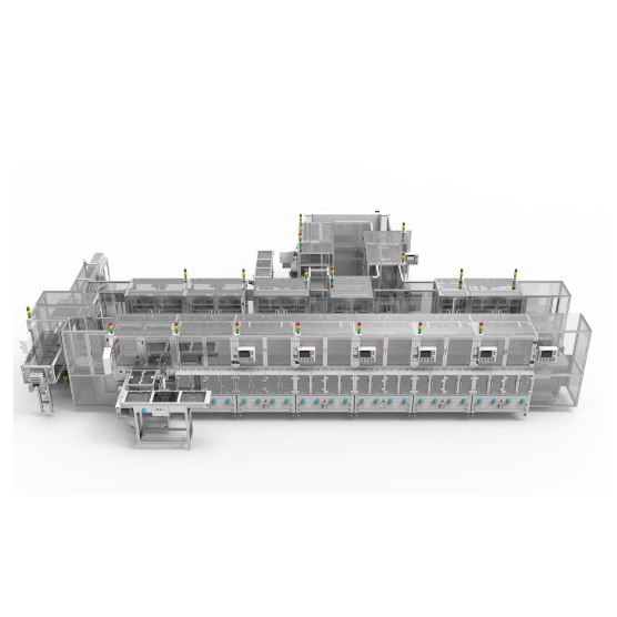
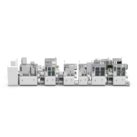
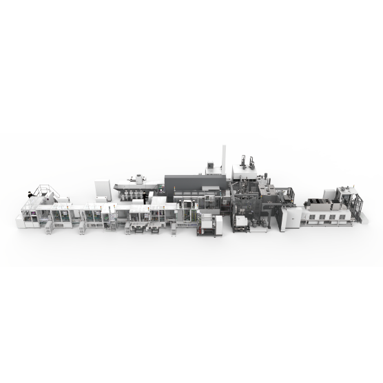
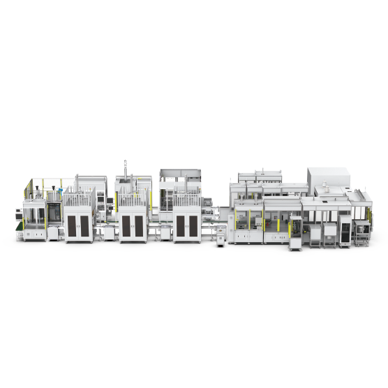
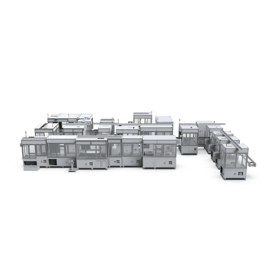
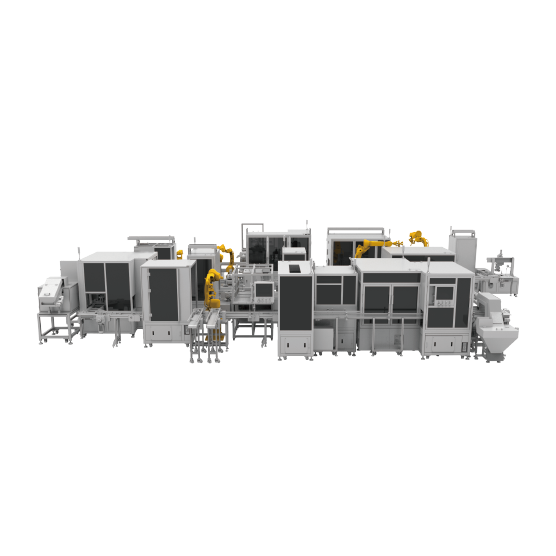
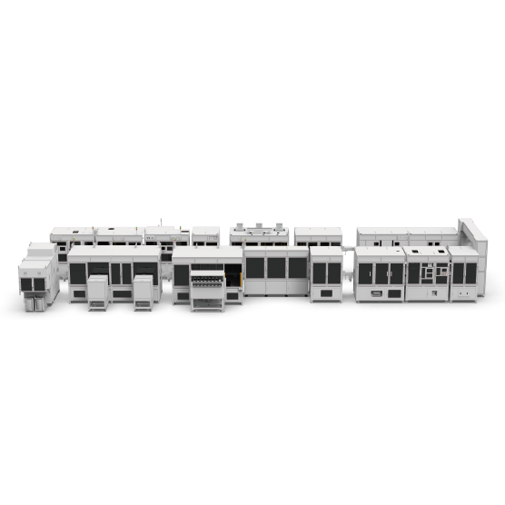
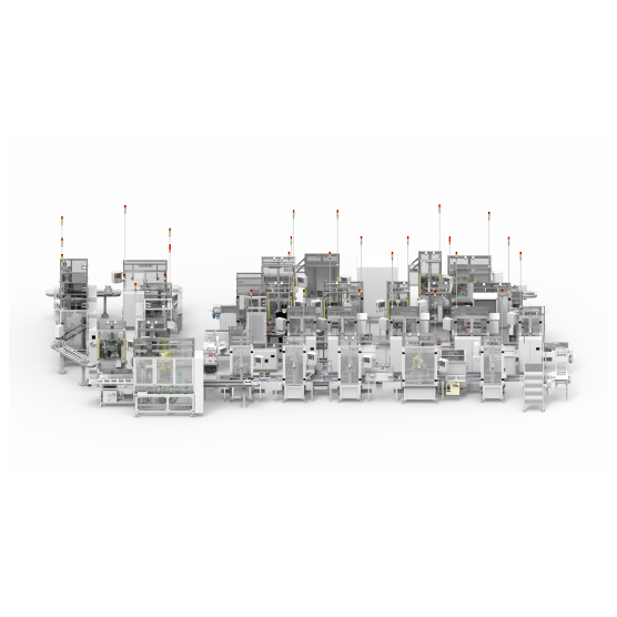
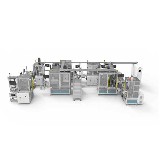
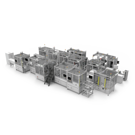
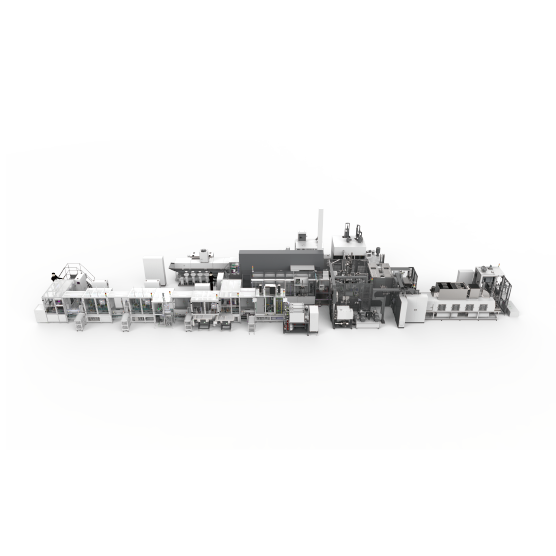
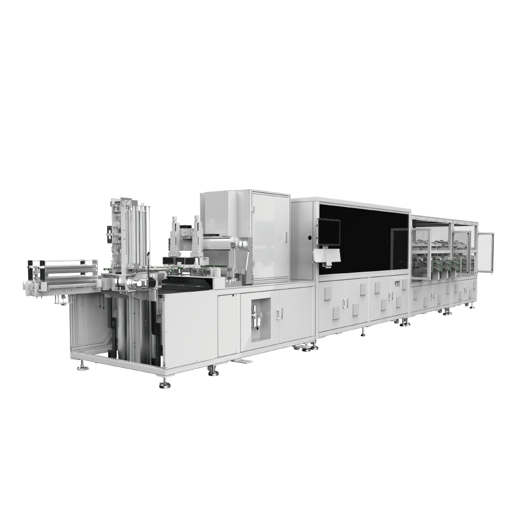


TB1500
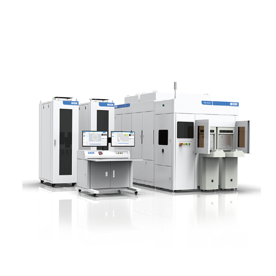
For 55-40 nm technology nodes
Compatible with 8-inch/12-inch wafers
Compatible with 8-inch/12-inch wafers
Scroll to explore
Advantages
-
High Sensitivity
-
High Throughput
-
Intelligent Software Support
-
Independent & Controllable Supply Chain
-
 High Sensitivity
Defect detection down to 60 nm
Advanced signal processing for enhanced signal-to-noise ratio
Broadband illumination for comprehensive defect capture

-
 High Throughput
High data rate
Multiple pixel size options
Optimized for high-speed scanning
-
 Intelligent Software Support
Online Smart Defect Classification (SDA)
Process Window Verification
Design Care Area Support
-
 Independent & Controllable Supply Chain
High-Throughput DUV Imaging System
High-speed deep ultraviolet TDI Camera
High-power LSP light source
Ultra-Precision Motion Stage