


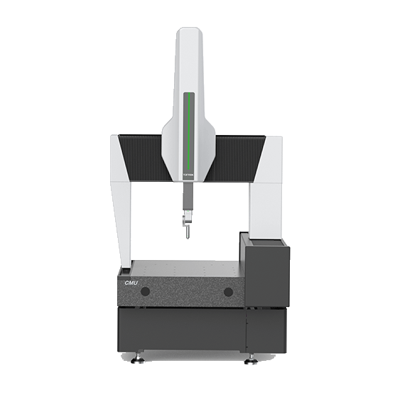
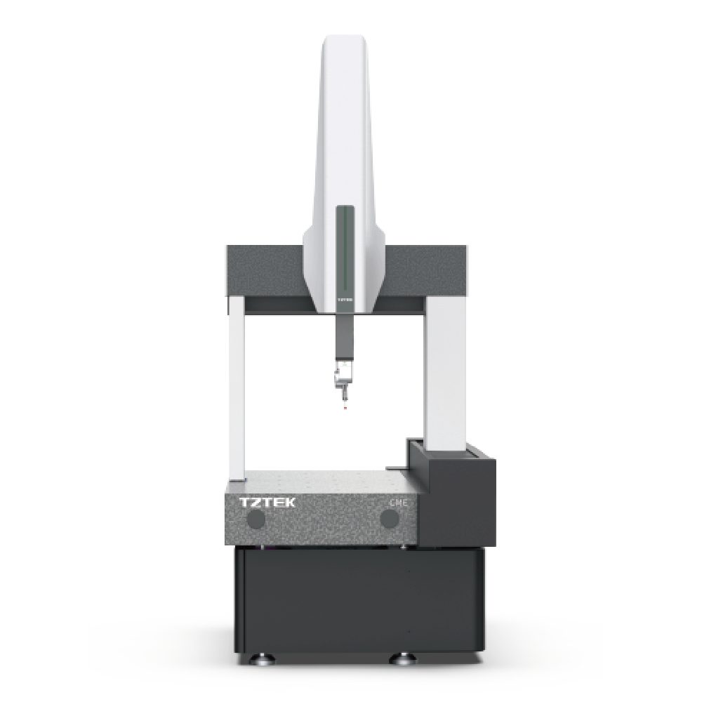
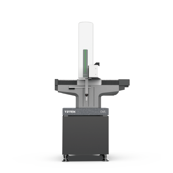
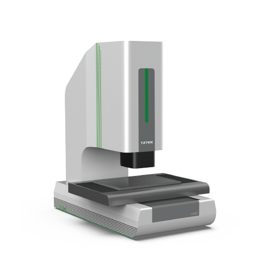


Mask Metrology & Inspection
INDUSTRY CHALLENGES
-
 01
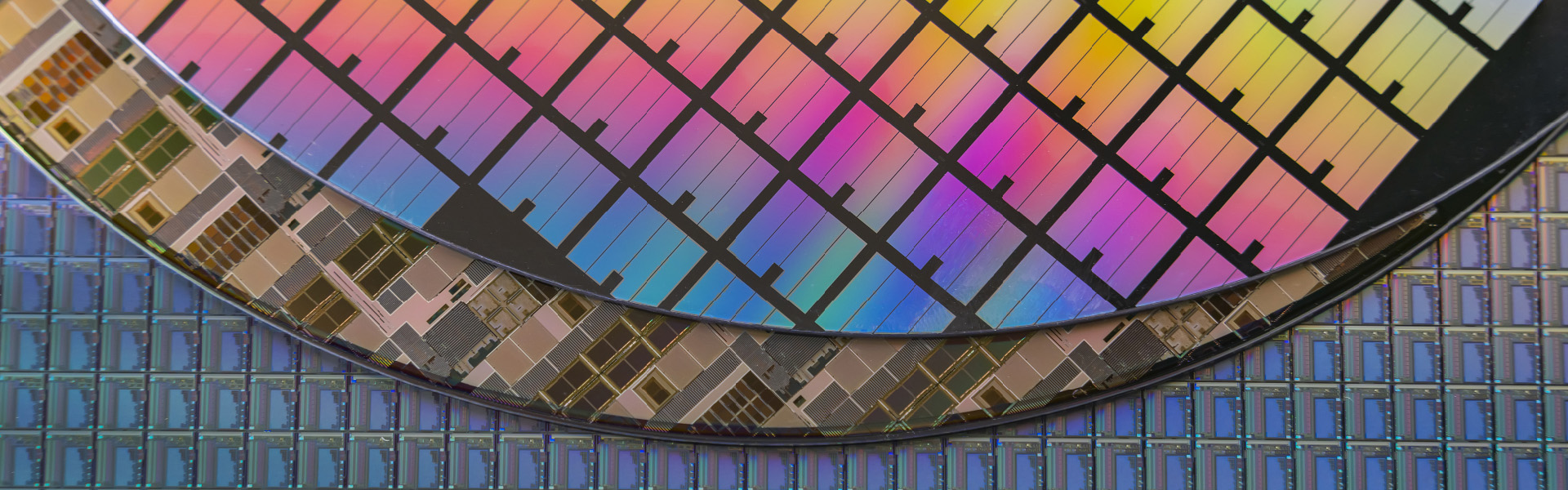
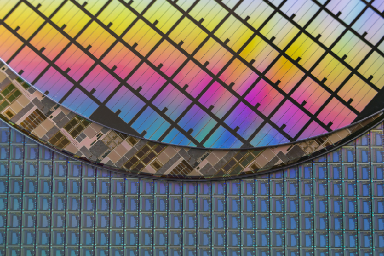
01Defect Replication Risk: A single photomask defect can be replicated across thousands of wafers, causing significant yield loss.
-
02
Demanding Inspection of Large, High-Density Patterns: Large-format photomasks and densely packed patterns demand high inspection sensitivity and defect detection capability.


INDUSTRY SOLUTION
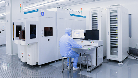
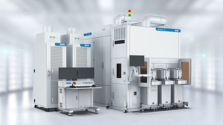
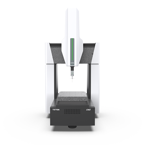
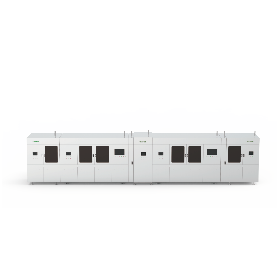
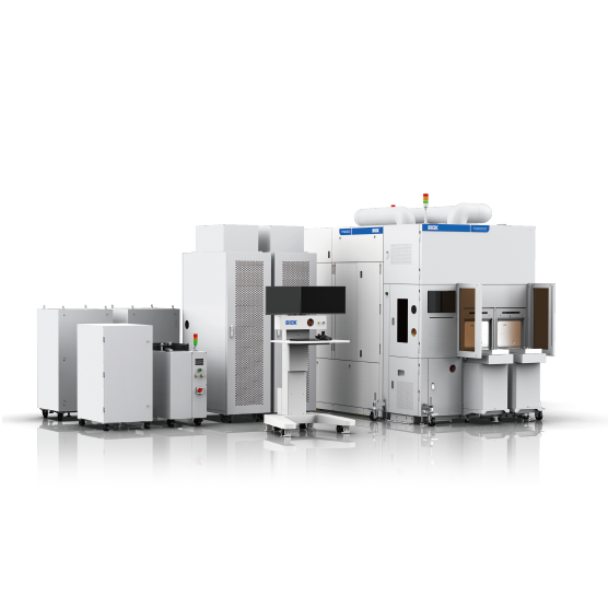
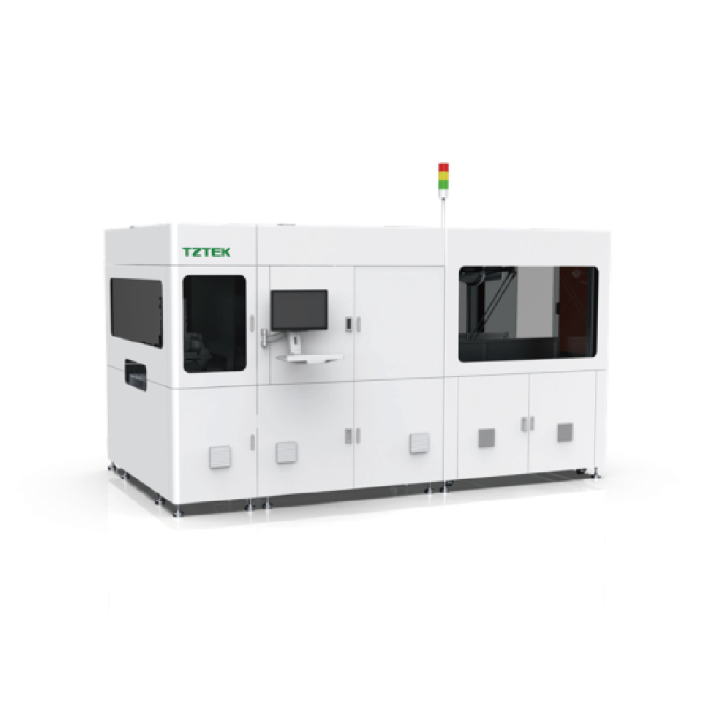
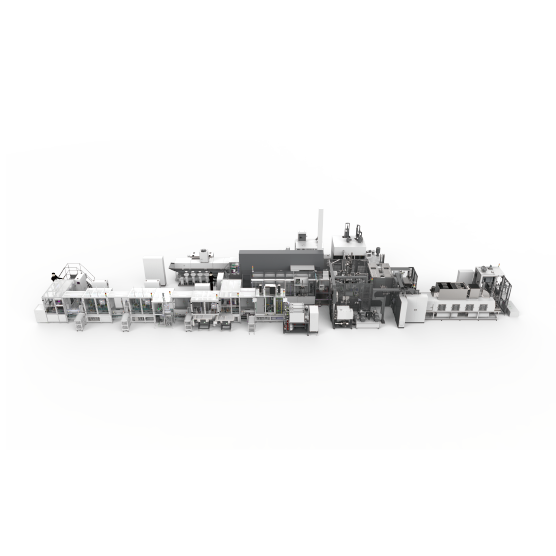
As semiconductor geometries continue to shrink, photomask manufacturing demands tighter CD control and higher defect sensitivity. TZTEK provides an integrated CD metrology and defect inspection solution for advanced photomask manufacturing, supporting automated, cleanroom-compatible production.
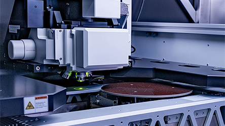
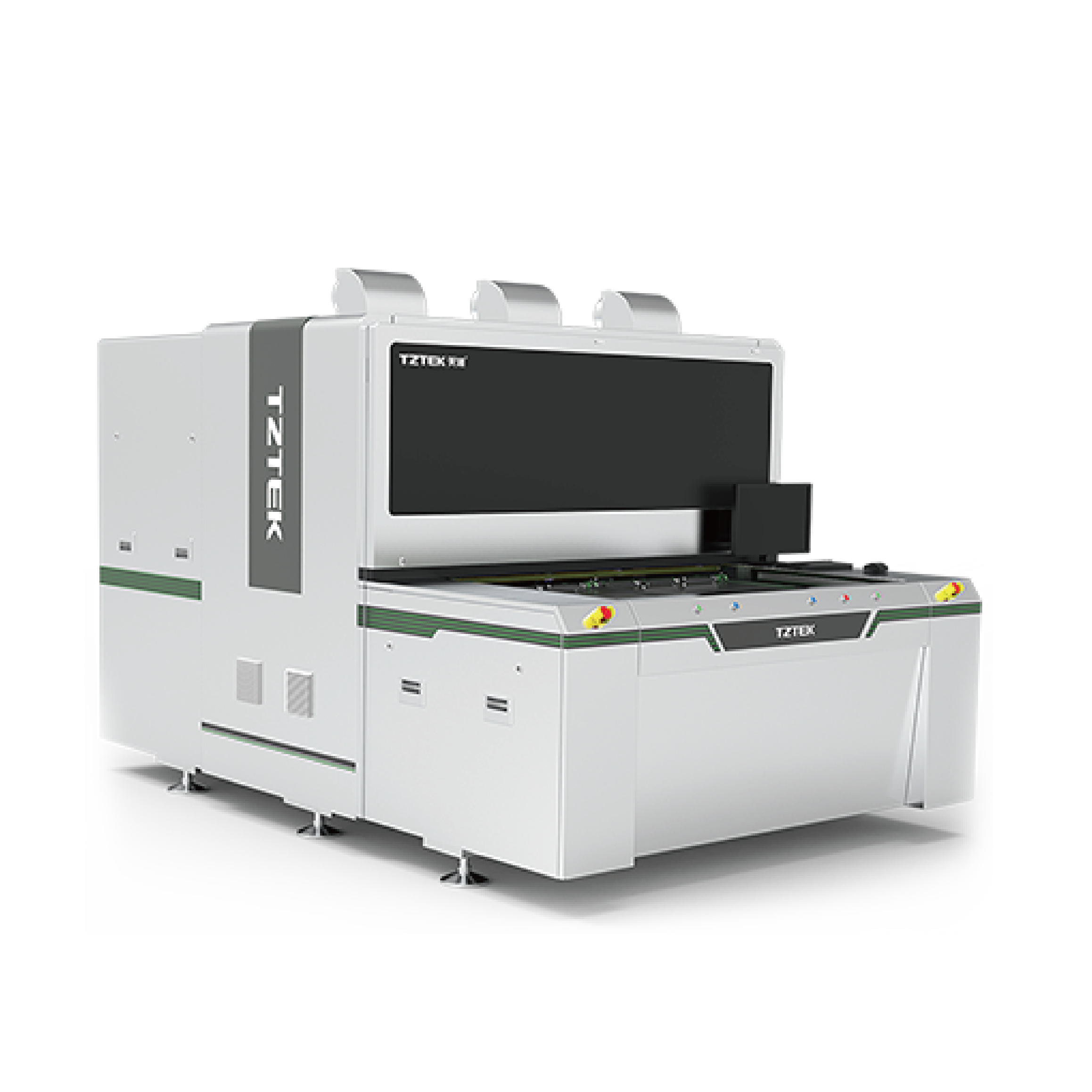
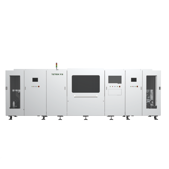
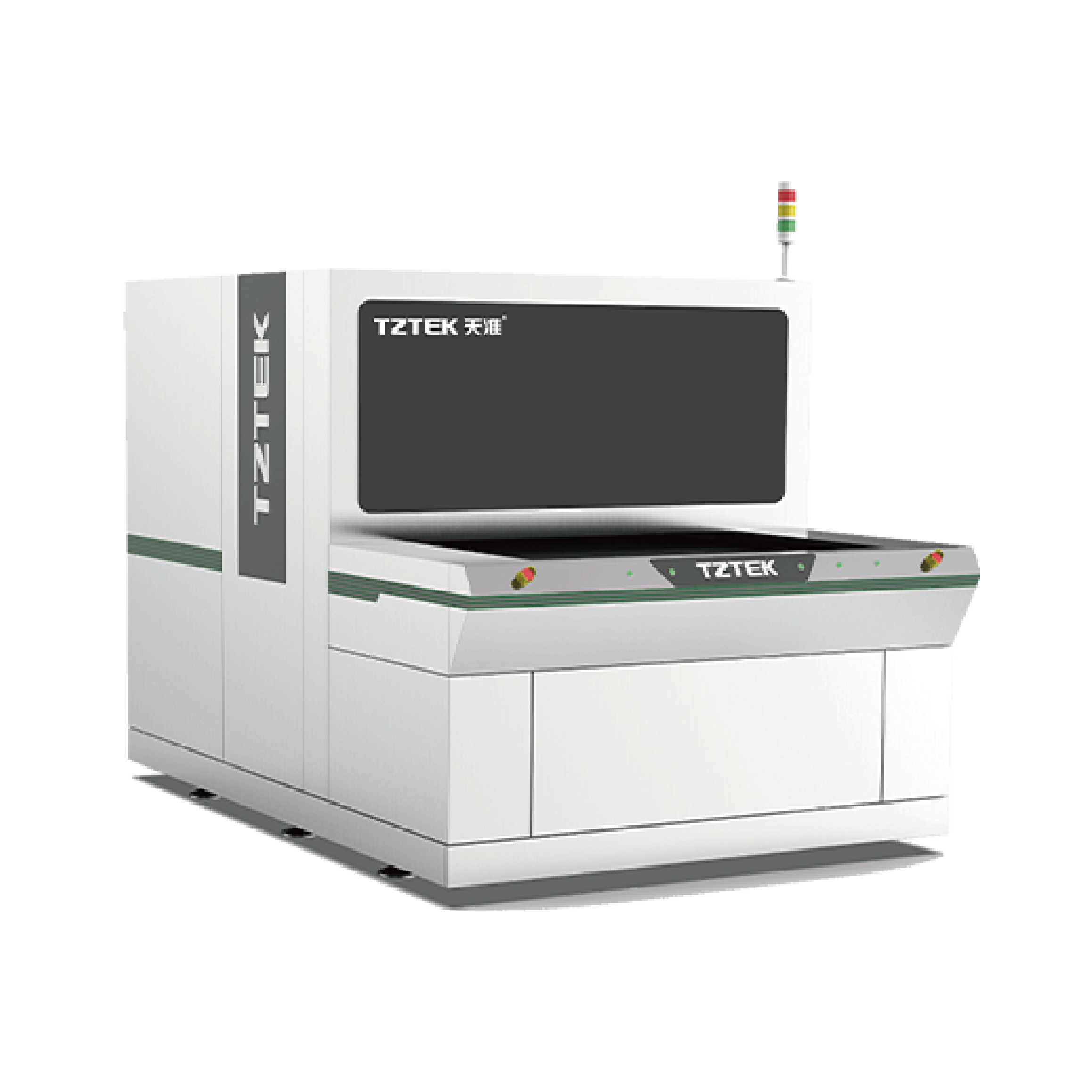
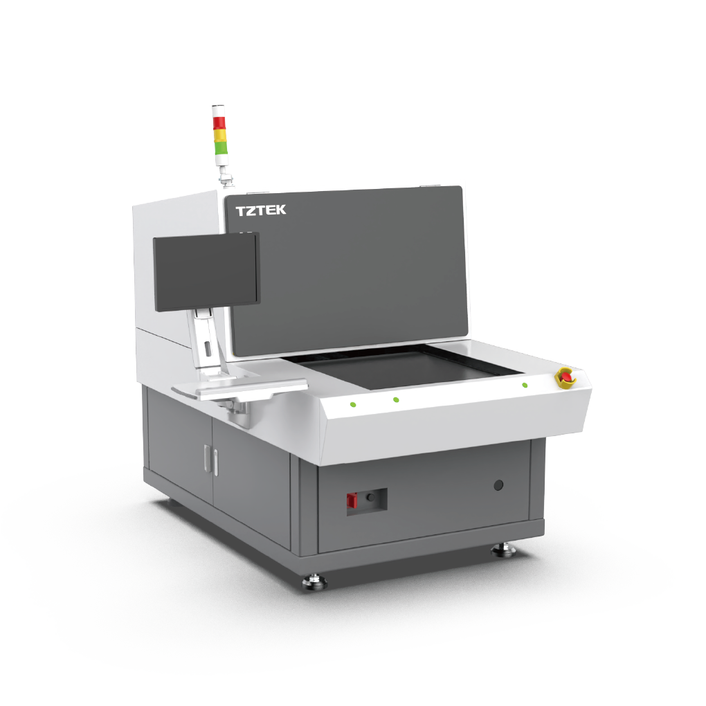
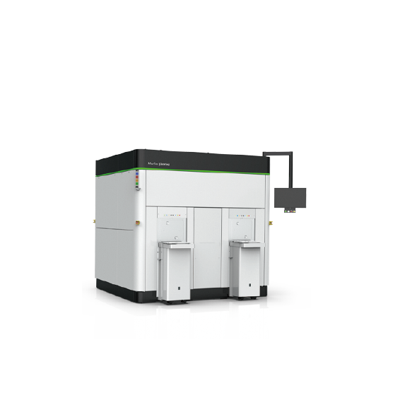
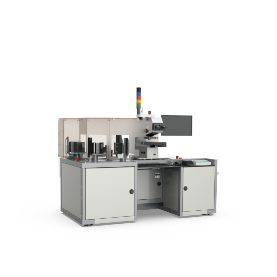
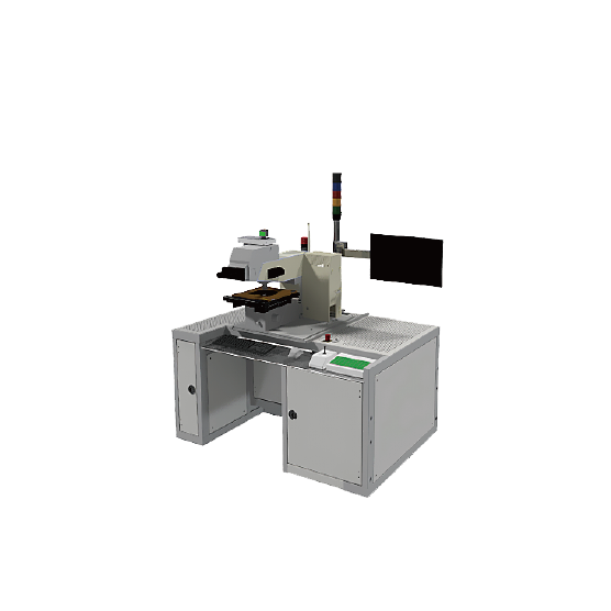
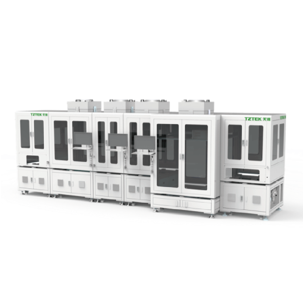
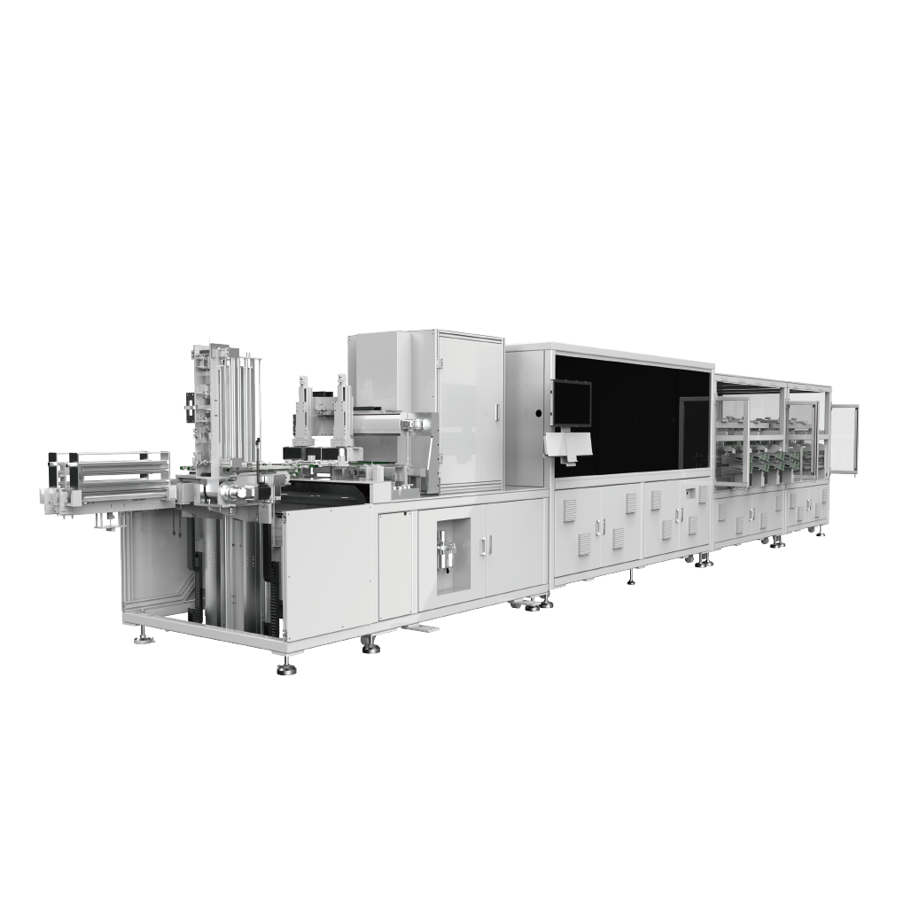
CD Metrology: MT270UV leverages UV optical metrology to provide high-precision measurement for photomasks up to 9 inches, with CD repeatability down to 1.5 nm. DaVinci 270UV features a fully enclosed, fully automated design.
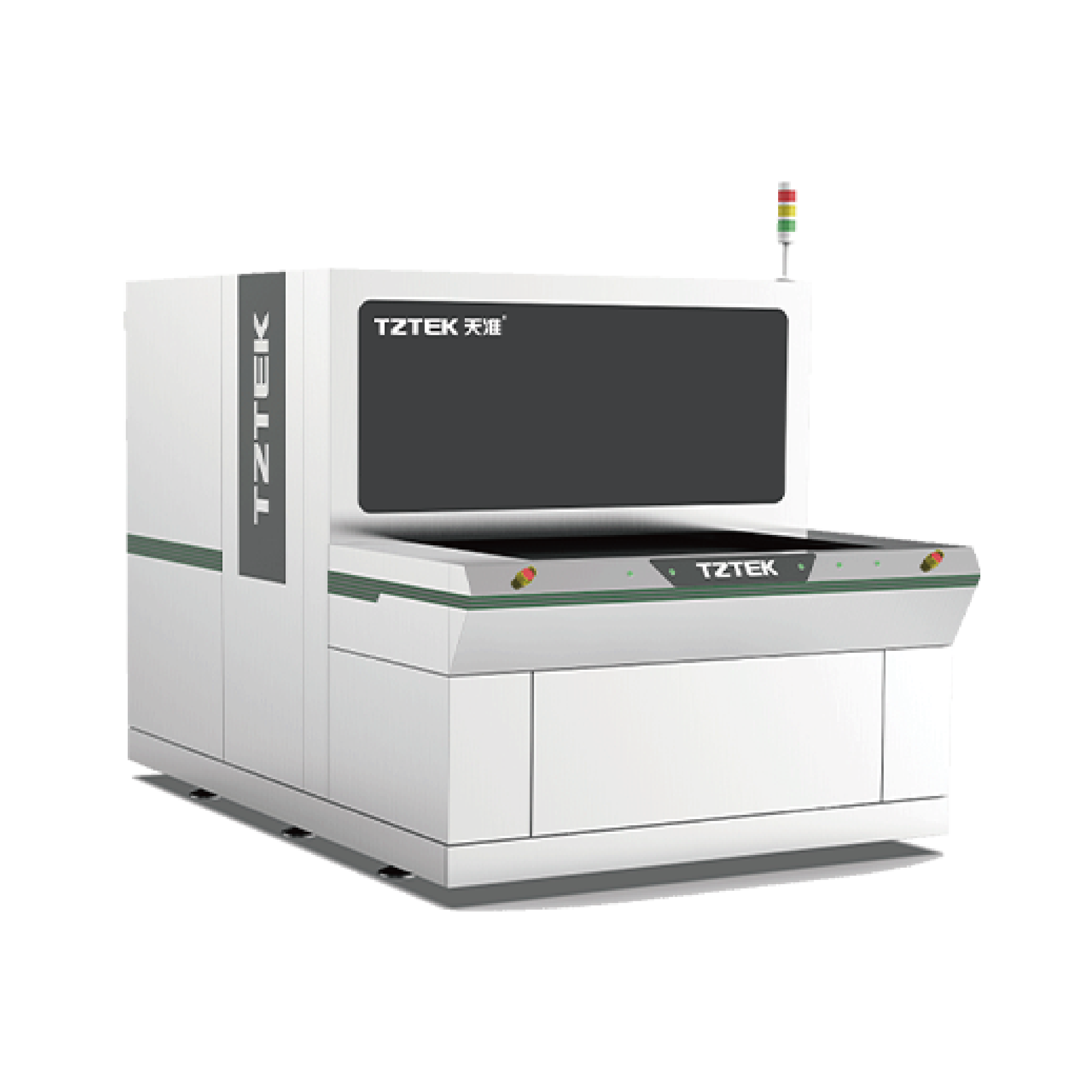
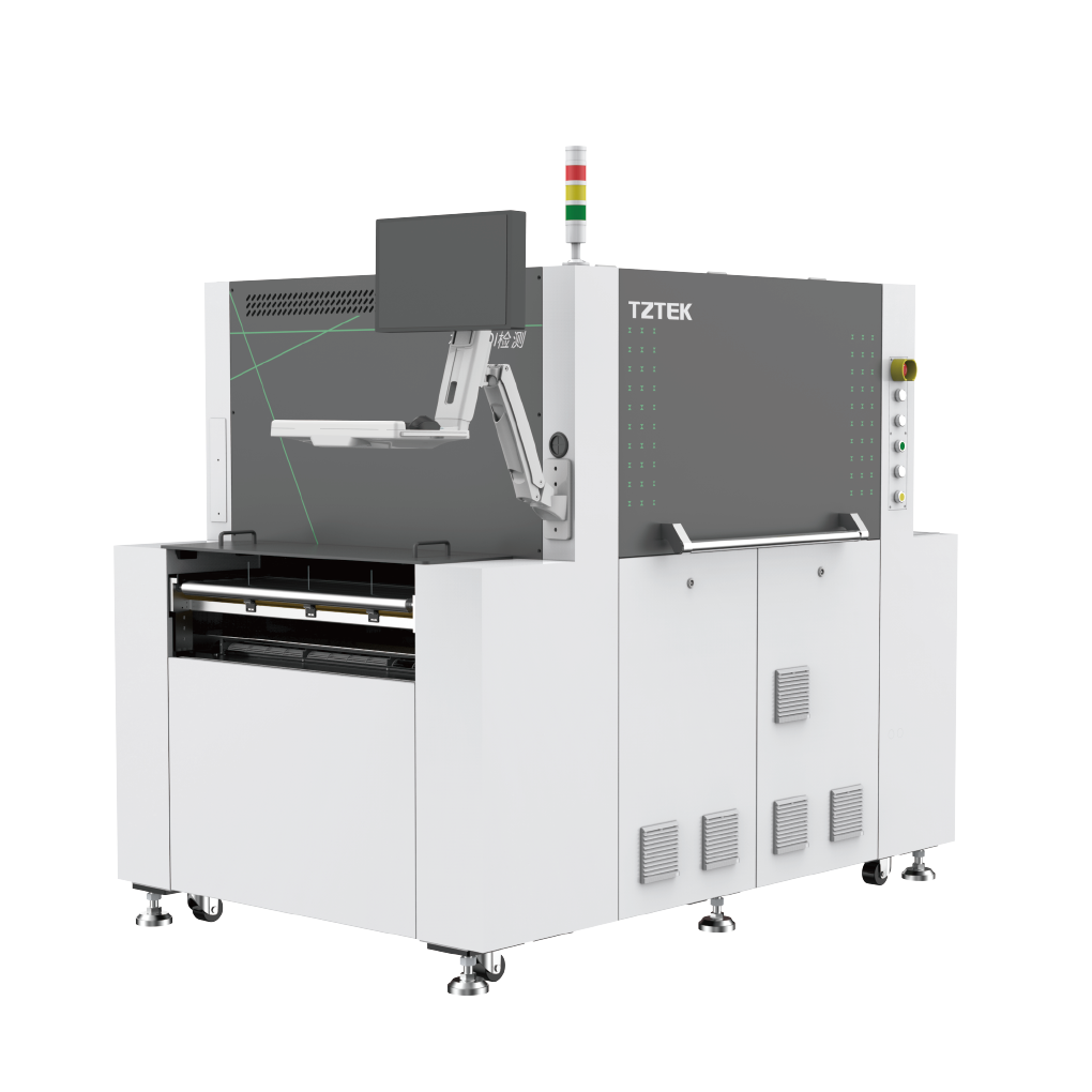
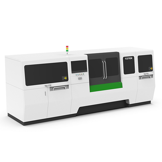
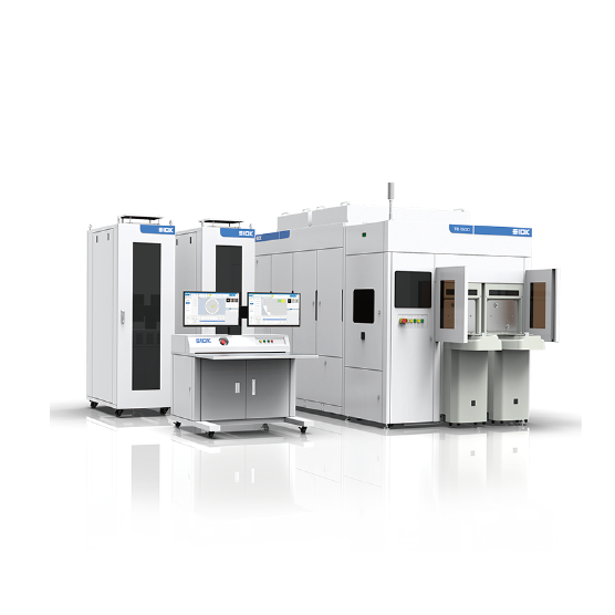
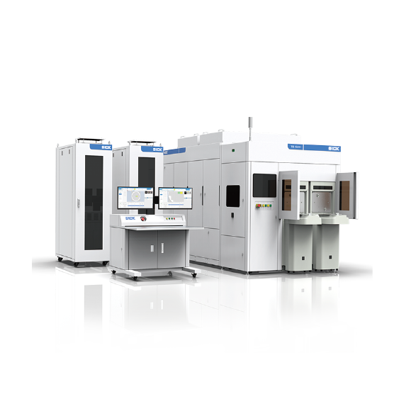
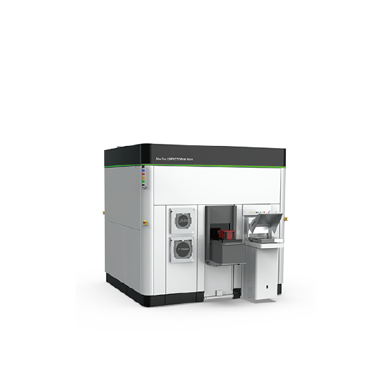
Defect Inspection: SPECTOR series (SPECTOR-M/A/5500) supports die-to-die and GDS-based comparison, detecting defects down to 0.8 μm on photomasks up to 14 inches. With CD repeatability <2 nm, typically <1 nm, plus SMIF, SECS/GEM, and automated handling, it supports automated manufacturing in cleanroom environments.
KEY ADVANTAGES
-


High-Precision Metrology: CD measurement repeatability down to 1 nm.
-

Flexibility: GDS support, recipe-free defect comparison, SMIF compatibility, automated handling.
-

Reliability & Low COO: Easy maintenance, no short-cycle consumables, long-term stable operation.