


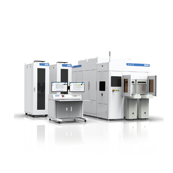
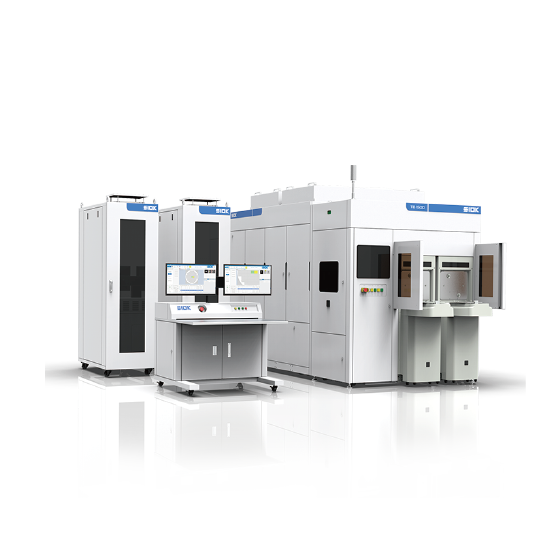
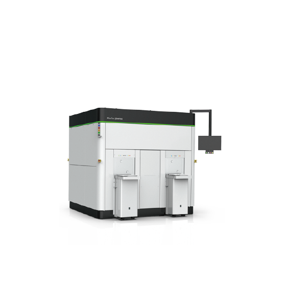
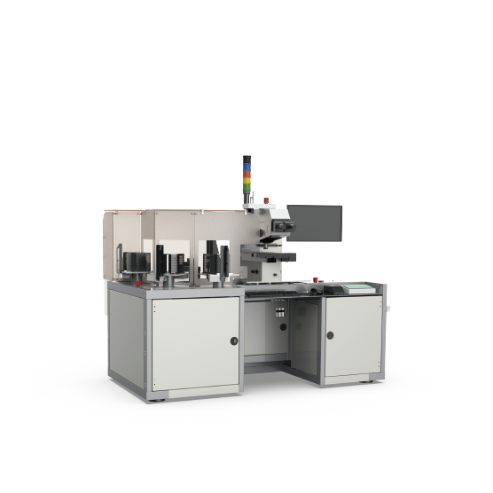
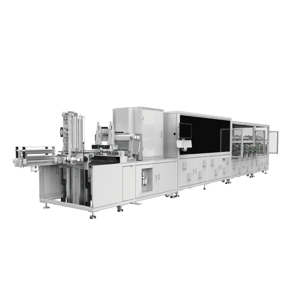


SEMICONDUCTORS — DELIVERING ADVANCED PROCESS CONTROL EQUIPMENT FOR AI CHIP MANUFACTURING
SEMICONDUCTOR MANUFACTURING CHALLENGES
-
 Advanced Node Scaling
Shrinking technology nodes demand higher-sensitivity defect inspection and more precise overlay and critical dimension (CD) metrology.
-
 Increasing Process Complexity
Emerging materials, device architectures, packaging, and heterogeneous integration require metrology and inspection solutions capable of supporting diverse processes and applications.
-
 Yield Optimization
Tighter process windows make comprehensive inspection and process control essential for improving yield.
-
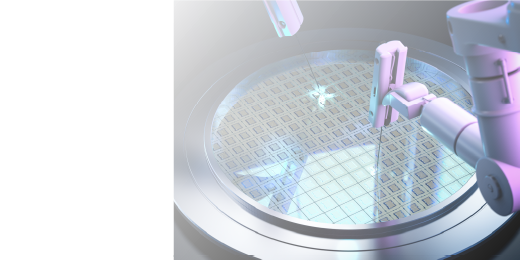 High-Volume Manufacturing
High-volume production demands nanometer-level precision, high throughput, and long-term measurement stability.


SOLUTIONS FOR
KEY SEMICONDUCTOR MANUFACTURING APPLICATIONS
-

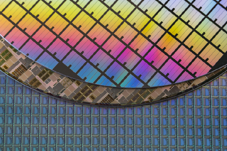 Photomasks
 -
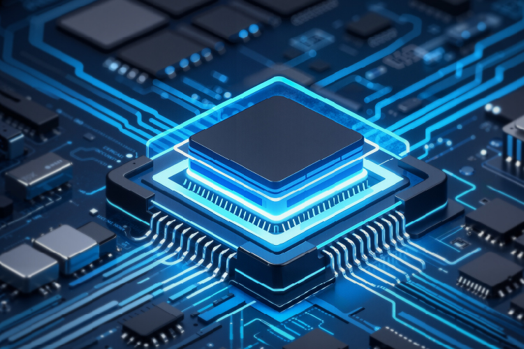 Advanced Packaging
 -
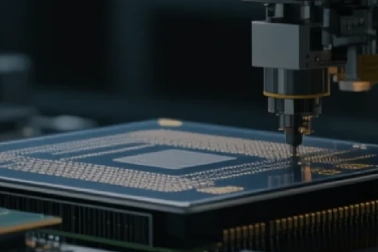 Power Devices
 -
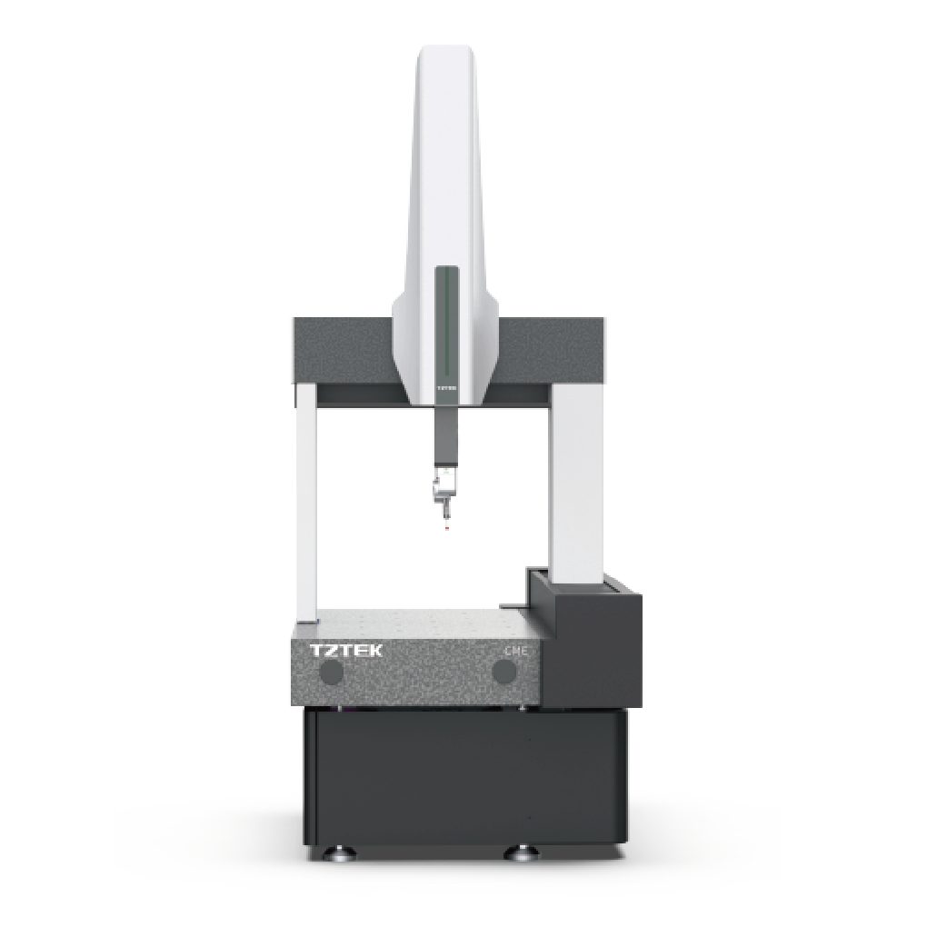
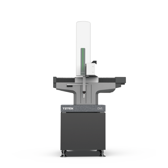
 Semiconductor Equipment Component Metrology

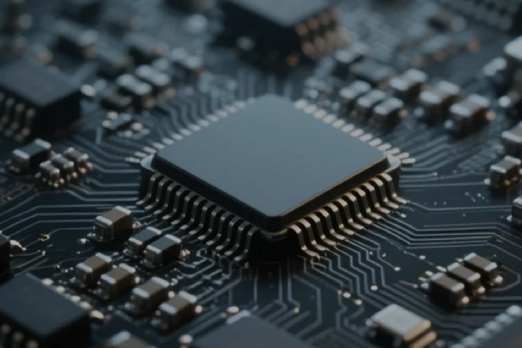
CORE CAPABILITIES


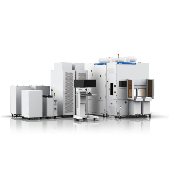
Combining ultra-precision optical systems, nano-scale motion control, and advanced AI algorithms, TZTEK delivers high-sensitivity inspection and nanometer-level metrology.

Designed for advanced nodes and advanced packaging, TZTEK provides inspection and metrology solutions for diverse materials, device structures, and critical process steps.

Proprietary industrial AI and data analytics enable intelligent defect inspection, real-time process monitoring, and yield optimization.

Enabling high-throughput inspection, automated operation, and closed-loop data management to meet the demands of advanced semiconductor manufacturing.


RELATED NEWS