






News
Sep 03, 2026
Industry Solution: High-Precision Quick Measurement for Stencil Aperture Position of Solder Paste Printing


As electronic manufacturing continues to evolve toward miniaturization and higher density, component dimensions keep shrinking while PCB integration increases, imposing stricter requirements on SMT solder paste printing stencil accuracy.
As a critical tool for solder paste printing, stencil aperture size and position directly affect solder joint quality, product yield, and reliability. Nowadays, stencil apertures are down to tens-of-micrometers range, and a single stencil can contain thousands to tens of thousands of micro-apertures. Achieving high-precision, high-efficiency inspection of massive micro-aperture over a large‑format area has become a key challenge for advancing precision electronics manufacturing capabilities.
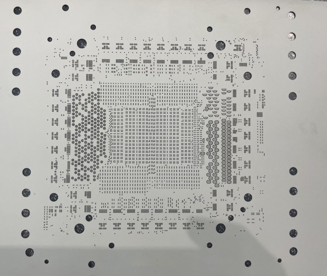
Industry Challenges: Dense Micro‑Apertures and Global Deformation — Bottlenecks in Stencil Inspection
For SMT manufacturing, stencil inspection lays the foundation for consistent solder‑paste printing and improved soldering yield. A leading precision electronics manufacturing service provider needed to perform full inspection of aperture size, position, and overall deformation during mass production of SMT stencils, and compare the results against Gerber design files to verify solder paste printing quality. However, as stencil fabrication precision improves, traditional inspection solutions reveal multiple limitations:
Limited Micro-Aperture Inspection Accuracy
Minimum aperture diameters fall below 0.1 mm, and ordinary optical equipment with limited resolution struggles to accurately capture micro-aperture dimensions and contour features.
Insufficient Inspection Efficiency for Large Formats
Traditional equipment cannot simultaneously deliver long travel range and high precision. Whole-board inspection requires hundreds of image stitching operations, resulting in long cycles and low efficiency.
Limited Capability for Correlating Design Data
Lack of automatic Gerber file comparison and global deformation analysis leads to low alignment efficiency.
Full Inspection Unable to Keep Pace with Production Takt Time
Massive aperture arrays require individual programmed measurement. The complex inspection workflow makes it difficult to meet high-takt production demands.
Technical Solution: Hardware‑Software Synergy to Deliver High‑Precision Stencil Metrology
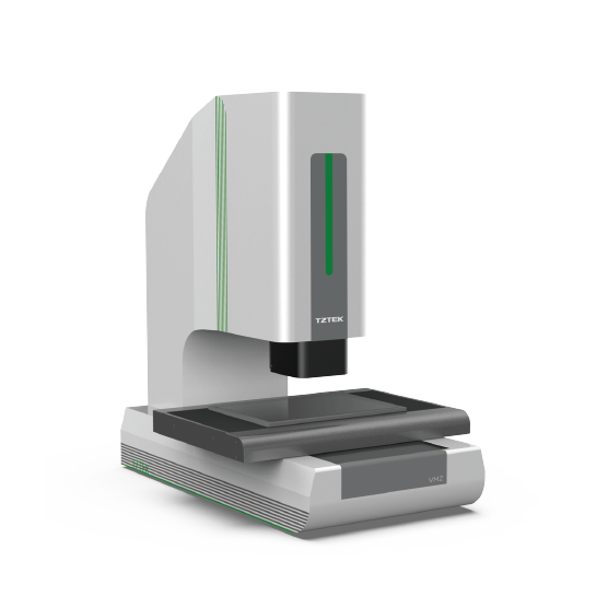
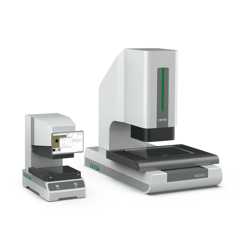
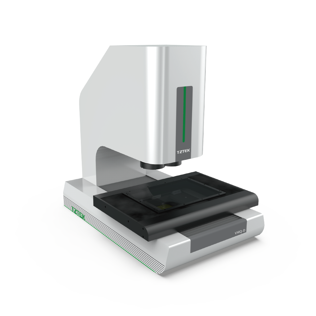
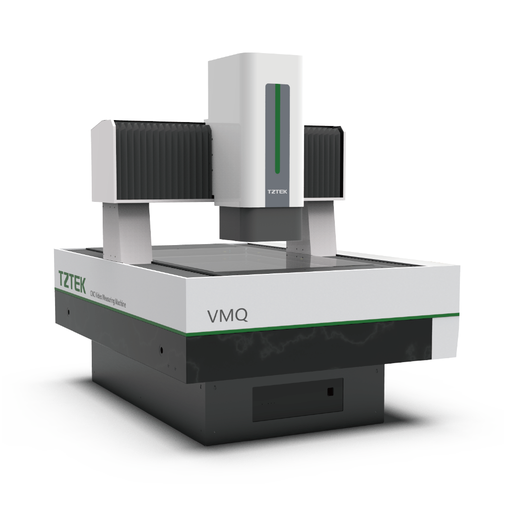
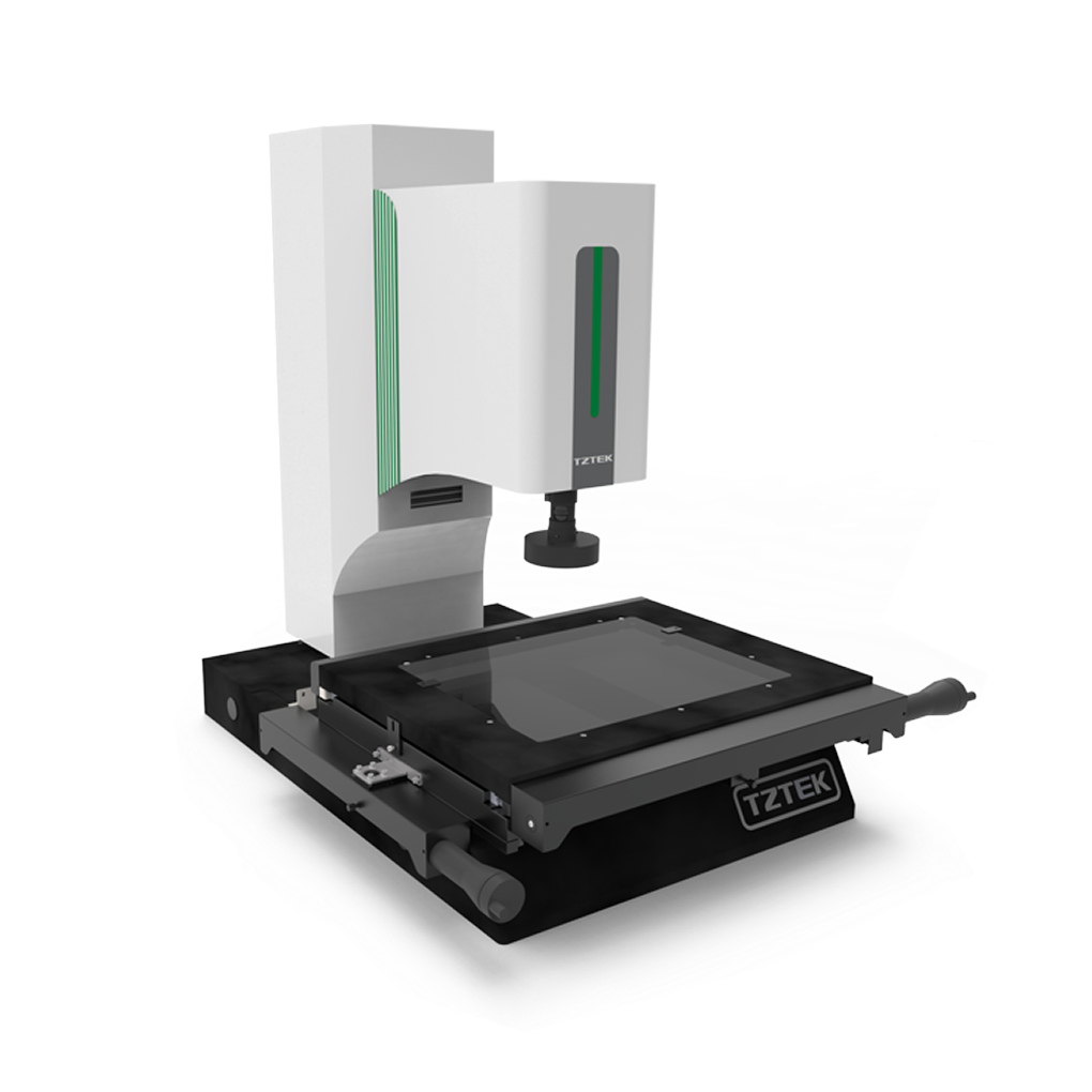
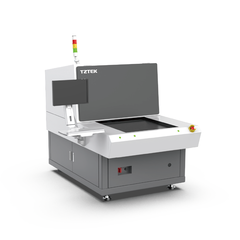
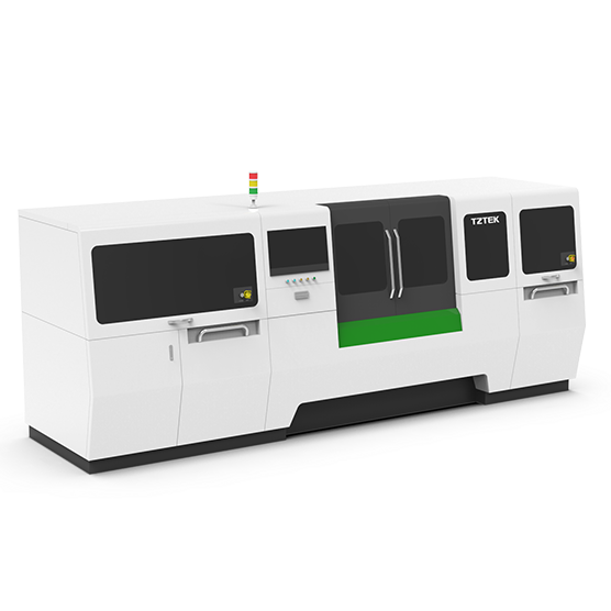
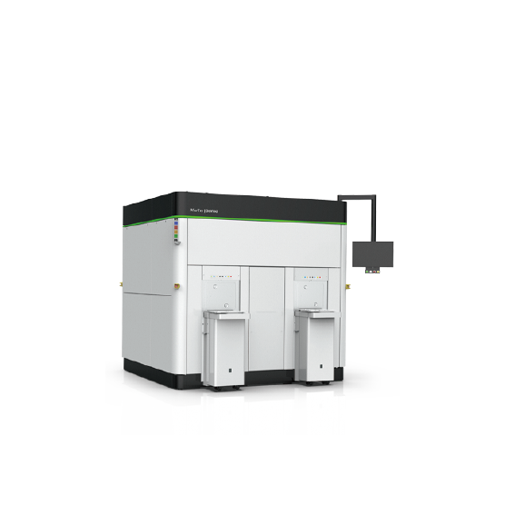
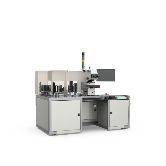
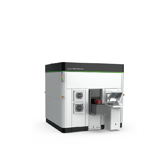
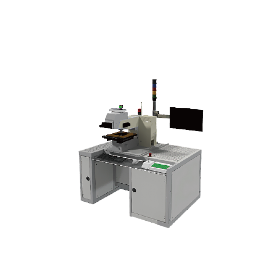
To address inspection demands for high‑accuracy, large‑size, high‑density apertures on SMT stencils, TZTEK has built an efficient measurement solution based on the VMQ quick video measuring machine and Vispec software. Through high-precision imaging and sensor fusion measurement technologies, it achieves simultaneous improvements in full inspection efficiency and accuracy for stencils.
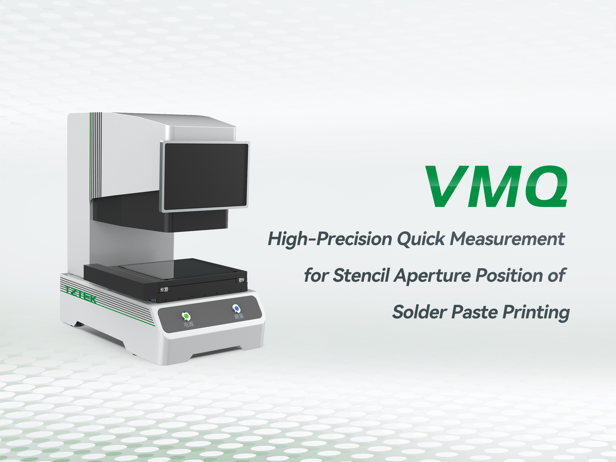
1. Dual-Magnification Imaging and Intelligent Optical Configuration for Both Wide Field of View and Micro-Aperture Measurement
Equipped with TZTEK's in-house dual-magnification lens, VMQ can capture both the stencil frame locating holes and micro-apertures smaller than 0.1 mm in a single shot, combining wide field of view with micrometer-level measurement precision.
To handle high reflectivity of stainless‑steel stencils, the system combines telecentric illumination and height‑adjustable epi‑illumination to accurately capture aperture wall contours while eliminating burr interference. It also reliably identifies fiducial marks and surface characters, ensuring alignment accuracy and imaging quality.
2. Intelligent Calibration and Fusion Measurement with Direct Gerber/CAD Import
The system supports direct import of Gerber/CAD design files and automatically generates theoretical measurement paths, ensuring measurement points align with design requirements. After loading, the system automatically recognizes fiducial marks or frame features, rapidly establishes the workpiece coordinate system, and automatically completes coordinate system calibration.
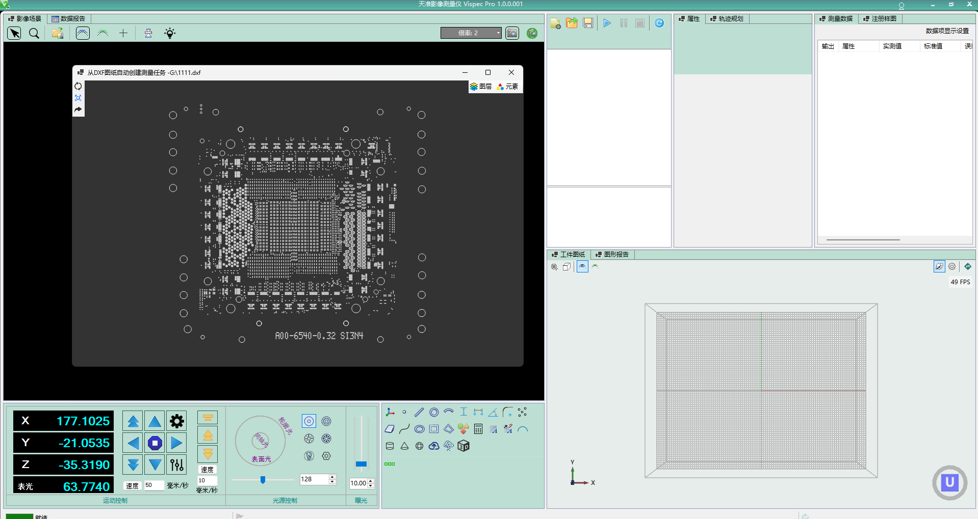
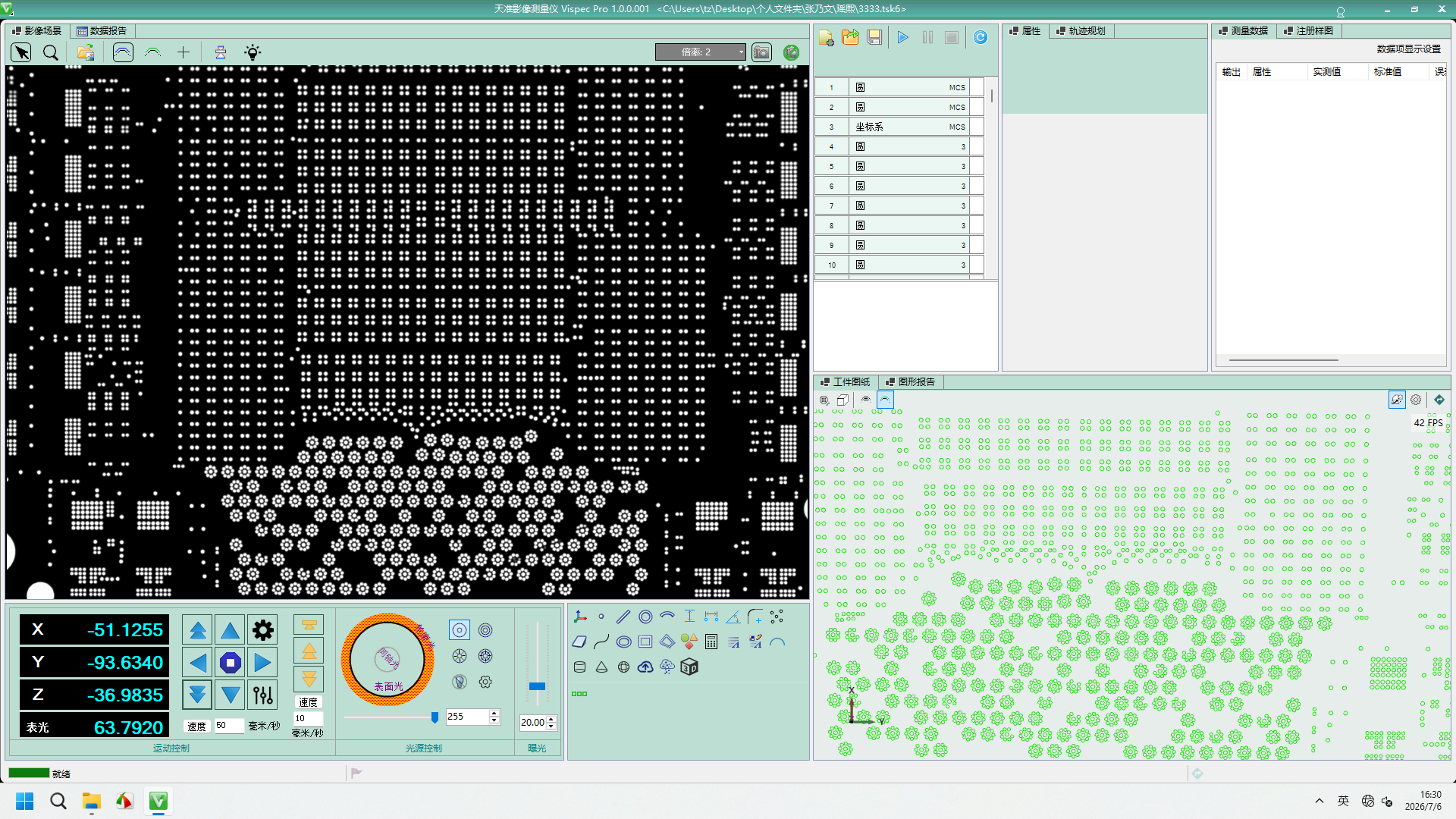
The measurement phase employs fusion measurement technology. The equipment continuously captures images during motion and automatically stitches them into high-resolution panoramas through sub-micrometer-level image registration algorithms. By simply defining scan paths that cover the stencil's key regions, all aperture data can be extracted from the panorama in a single pass, delivering over 20% efficiency improvement compared to traditional point-by-point measurement. For extra-large stencils, the system supports high-precision zonal scanning with automatic data fusion and automatically generates complete measurement reports.
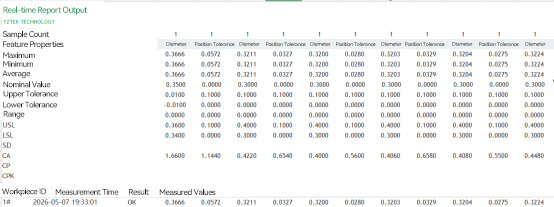
Value Creation: Improved Full Inspection Efficiency and Continuously Refined Quality Loop
After solution deployment, the customer achieved simultaneous improvements in stencil inspection efficiency and quality management capabilities:
- Whole-board full inspection cycle reduced from several hours to minute-level. No need for dedicated custom fixtures, dramatically compressing stencil changeover time.
- Micron‑level requirements for aperture dimension and positional tolerance are satisfied, and aperture‑alignment consistency is significantly enhanced.
- Complete traceability of full‑volume inspection data provides reliable inputs for SPC analysis and stencil service‑life prediction.
This solution not only satisfies the customer's high-takt mass production requirements for SMT lines, but also further enhances solder paste printing consistency and subsequent reflow yield, providing more stable quality assurance for precision electronics manufacturing.
As precision electronics manufacturing continues to evolve toward higher density and miniaturization, efficient and intelligent industrial measurement is becoming a critical foundational capability for manufacturing upgrades. TZTEK continues to deepen its presence across the AI industry chain, empowering customers to improve manufacturing precision, product yield, and production efficiency with high-end measurement and inspection equipment. To learn more about high-precision measurement solutions for the precision electronics manufacturing industry, please contact TZTEK.
MORE NEWS
-
News
Sep 03, 2026
Industry Solution: High-Precision Quick Measurement for Stencil Aperture Position of Solder Paste Printing -
News
Aug 03, 2026
Share Donation Valued at Over RMB 600 Million Completed: TZTEK Controlling Shareholder Empowers AI Research and Basic Education Development -
News
Jul 31, 2026
Boosting Efficiency for Large-Size Precision Measurement: TZTEK VMG Gantry Video Measuring Machine Gets Comprehensive Upgrade
